The NOR Gate: How It Built Apollo and Powers Modern Logic
The Apollo Guidance Computer was built almost entirely from NOR gates. Functional completeness, reliability via uniformity, and CMOS-implementation limits.

TL;DR: The NOR gate outputs 1 only when all inputs are 0 (). Like NAND it is functionally complete — every Boolean function can be built from NOR alone. The Apollo Guidance Computer used about 5,600 NOR gates and nothing else. In modern CMOS, NOR’s series-PMOS pull-up is slower than NAND’s series-NMOS pull-down, which is why NAND dominates today’s standard cell libraries.
The NOR gate is the universal constructor that built the Apollo Guidance Computer (AGC), the digital brain of the lunar missions. The AGC used about 5,600 NOR gates — every flip-flop, every adder, every register, every interrupt path was implemented from a single dual-3-input NOR-gate IC. The choice was not arbitrary: it was driven by reliability through uniformity, the universality of NOR logic, and the technological constraints of the 1960s.
Defining the NOR Gate: The All-Zero Detector
At its simplest level, a NOR gate (NOT-OR) is a digital logic gate that implements logical negation of the OR operation. Its output is HIGH (logic 1) if and only if all of its inputs are LOW (logic 0). If any input is HIGH, the output is immediately pulled LOW.
Think of it as a gate that asks a very specific question: “Are all participants silent?” If the answer is yes, it speaks. If even one person makes noise, it shuts down. This “all-zero detection” is more powerful than it looks on the surface.
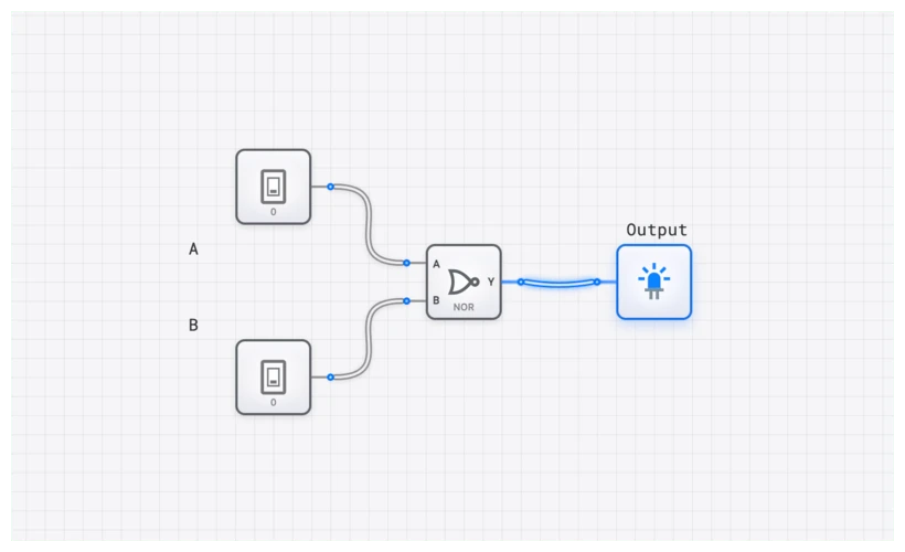
Technical Specification: The Truth Table
The behavior of a 2-input NOR gate is elegantly captured by its truth table. In digisim.io, you can verify this by placing a NOR component and toggling two INPUT_SWITCH components.
| Input A | Input B | Output Y |
|---|---|---|
| 0 | 0 | 1 |
| 0 | 1 | 0 |
| 1 | 0 | 0 |
| 1 | 1 | 0 |
The Boolean Foundation
In Boolean algebra, the NOR operation is expressed as the OR operation followed by a NOT operation. We represent this using the overline notation for negation:
Applying De Morgan’s theorems reveals the NOR gate’s “hidden personality” — useful for circuit minimization:
This expression tells us that a NOR gate is logically equivalent to an AND gate with inverted inputs. This duality is why we can use NOR gates to build any other logic function imaginable.
The Apollo Connection: NOR Gates on the Moon
In the early 1960s, the MIT Instrumentation Laboratory faced a monumental task: building a computer small enough to fit on a spacecraft, reliable enough to survive launch vibrations, and powerful enough to navigate to the Moon and back. At the time, integrated circuits (ICs) were in their infancy — the first commercial ICs had appeared only a year or two earlier.
The lead designer, Eldon Hall, made a radical decision. Instead of using a variety of different chips, the entire Apollo Guidance Computer (AGC) would be built from a single component: the Fairchild Micrologic 9912, a dual 3-input NOR gate IC in a flat-pack package.
Reliability Through Uniformity
By standardizing on one gate type, NASA could purchase them in massive quantities (the AGC program bought roughly 60% of all integrated circuits manufactured in the United States during 1963-1964) and subject them to punishing qualification testing: temperature cycling, vibration, radiation exposure, and accelerated life testing. If a batch of NOR gates passed qualification, every gate in the computer was trusted. If the team had used a mix of AND, OR, NOT, and flip-flop ICs from different manufacturers, the testing matrix would have exploded in complexity.
Inside the AGC
The AGC used approximately 5,600 NOR gates (2,800 dual-gate packages). Every flip-flop was built from cross-coupled NOR gates. Every adder was a NOR-gate tree. Every register, every counter, and every instruction decoder was a cluster of NOR gates wired according to the universality principle.
The computer had a 2.048 MHz clock, 2,048 words of erasable (RAM) memory, and 36,864 words of fixed (ROM) “rope memory.” It weighed 70 pounds and consumed 55 watts. By modern standards, it was extraordinarily limited. By 1960s standards, it was a miracle of miniaturization.
The 1202 Alarm
During the Apollo 11 lunar descent, the DSKY (Display/Keyboard) flashed a “1202” alarm — an executive overflow, meaning the computer was being asked to do more than it could handle in real time. The AGC’s priority-based interrupt system, implemented entirely in NOR gates, shed lower-priority tasks (rendezvous radar processing) and kept the critical navigation and guidance routines running. The NOR-gate interrupt logic saved the mission. Flight controller Steve Bales made the call: “We’re go on that alarm.” Armstrong and Aldrin landed safely.
The AGC’s Legacy
The AGC was not just a computer; it was proof that digital logic — specifically, NOR gate logic — could be trusted with human lives. It demonstrated that a single universal gate, manufactured to extreme reliability standards, could implement any computational function required for spaceflight. This principle of “reliability through simplicity” influenced military and aerospace computing for decades.
Proving NOR Universality: Building Every Gate from NOR
A gate is “universal” (functionally complete) if it can implement NOT, AND, and OR. Once you have those three, you can build any Boolean function, any combinational circuit, and any sequential circuit. Let’s prove NOR universality step by step.
1. NOT from NOR (1 gate)
Tie both inputs of a NOR gate to the same signal:
Since by the idempotence law, this simplifies to pure inversion.
2. OR from NOR (2 gates)
A NOR gate is an OR followed by a NOT. To undo the inversion, pass the output through a second NOR gate configured as an inverter:
Construction: Feed and into the first NOR gate. Feed the output into both inputs of a second NOR gate.
3. AND from NOR (3 gates)
Apply De Morgan’s theorem: . We need to invert both inputs, then NOR the results:
Construction:
- Gate 1 (inverter): Both inputs tied to . Output is .
- Gate 2 (inverter): Both inputs tied to . Output is .
- Gate 3: Inputs are and . Output is .
4. NAND from NOR (4 gates)
Since , we invert both inputs and then OR them. The NOR-based OR uses 2 gates, and the two inverters use 2 gates, for a total of 4:
- Gates 1-2: Invert and (two NOR-as-inverter gates).
- Gate 3: NOR the inverted inputs: . Wait — that gives AND, not NAND. Instead, we need to OR the inverted inputs. Use Gate 3 as a NOR on the inverted inputs, and Gate 4 as an inverter on Gate 3’s output.
5. XOR from NOR (5 gates)
This is a useful exercise. The XOR function can be restructured. One efficient NOR-only implementation uses 5 gates:
- Gate 1:
- Gate 2:
- Gate 3:
- Gate 4: — this is XNOR, not XOR yet.
- Gate 5: — used as an inverter, producing the final .
Skipping Gate 5 is a common mistake: the four-gate sub-network produces XNOR, and you need one more NOR-as-inverter to flip it to XOR. Try building both versions on digisim.io and verifying the truth tables with the OSCILLOSCOPE.
The NOR-Based SR Latch: Where Logic Meets Memory
The NOR gate’s most historically important application — beyond the AGC itself — is the SR Latch, the most fundamental memory element in digital electronics. Every flip-flop, every register, and every bit of SRAM is built on this principle.
Construction
An SR Latch requires just two NOR gates, cross-coupled so that the output of each gate feeds back into an input of the other:
- Gate 1 (the gate): Inputs are (Reset) and (the output of Gate 2).
- Gate 2 (the gate): Inputs are (Set) and (the output of Gate 1).
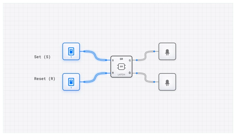
Operation
| S | R | Q | State | |
|---|---|---|---|---|
| 0 | 0 | Previous | Previous | Hold (memory) |
| 1 | 0 | 1 | 0 | Set |
| 0 | 1 | 0 | 1 | Reset |
| 1 | 1 | 0 | 0 | Forbidden |
How it works: When goes HIGH, Gate 2 sees a HIGH input and forces to 0. This 0 feeds back to Gate 1, which now has both inputs LOW (R=0, =0), so goes HIGH. Even after returns to 0, the feedback loop sustains the state: remains 1 because remains 0.
The forbidden state: When both and are HIGH simultaneously, both NOR gates see at least one HIGH input, forcing both and to 0. This violates the invariant that and must be complementary. When both inputs return to 0 simultaneously, the circuit enters a metastable race condition and may settle unpredictably. This is why higher-level circuits (D flip-flops, JK flip-flops) add logic to prevent this condition.
Building It on digisim.io
- Place two NOR gates side by side.
- Connect the output of Gate 1 to one input of Gate 2.
- Connect the output of Gate 2 to one input of Gate 1.
- Connect INPUT_SWITCH “S” to the free input of Gate 2.
- Connect INPUT_SWITCH “R” to the free input of Gate 1.
- Connect OUTPUT_LIGHT components to both outputs.
- Toggle S HIGH briefly, then return to LOW. Observe that Q latches to 1.
- Toggle R HIGH briefly, then return to LOW. Observe that Q resets to 0.
This is the exact same circuit topology used in every flip-flop inside the AGC. Approximately 5,600 NOR gates, cross-coupled in pairs, gave the Apollo computer its registers and counters.
CMOS NOR Gate: The Transistor-Level View
Understanding why NOR lost the silicon war to NAND requires looking at the CMOS implementation.
A 2-input CMOS NOR gate consists of:
- Pull-Down Network (PDN): Two NMOS transistors in parallel. If either input is HIGH, the output is pulled to ground. NMOS transistors in parallel have low resistance — this is fast.
- Pull-Up Network (PUN): Two PMOS transistors in series. Both inputs must be LOW for the output to be pulled to . PMOS transistors in series add resistance — this is slow.
The problem is that PMOS transistors have approximately 2-3x lower carrier mobility than NMOS transistors. When placed in series, their resistances add, making the pull-up (LOW-to-HIGH) transition significantly slower than the pull-down (HIGH-to-LOW) transition. To equalize rise and fall times, designers must make the PMOS transistors wider (larger), which increases capacitance and silicon area.
For a 2-input gate, the penalty is manageable. For a 3-input or 4-input NOR gate, the series PMOS stack becomes severe. The AGC used 3-input NOR gates, but in 1960s RTL technology, not CMOS, so this particular penalty did not apply. In modern CMOS, 3-input NOR gates are rarely used in performance-critical paths.
This is the fundamental reason NAND dominates modern CMOS standard cell libraries: the NAND topology places the fast NMOS transistors in series and the slow PMOS transistors in parallel — a more favorable arrangement.
Verification with the OSCILLOSCOPE
When building these circuits in digisim.io, don’t trust the OUTPUT_LIGHT alone. To see propagation delay and any glitches, use the OSCILLOSCOPE — see Propagation Delay: The Physics That Dictates Digital Speed for a full treatment.
- Place an OSCILLOSCOPE component.
- Connect Channel 1 to your input switch.
- Connect Channel 2 to the output of your NOR-based AND gate.
- Toggle the switch and watch the waveforms.
In a real physical circuit, you would see a tiny delay () between the input changing and the output responding. While digisim.io provides an idealized simulation, using the OSCILLOSCOPE helps you develop the habit of “timing-first” thinking, which is critical when you move on to complex components like the COUNTER_8BIT or the REGISTER_8BIT.
Curriculum Integration
If you’re following the structured learning path on digisim.io, the NOR gate appears at several critical junctures:
- De Morgan’s Laws and Boolean Algebra: This is where you will learn the mathematical proofs that make NOR universality possible.
- Universal Gate Construction: A deep dive into building complex logic using only NOR and NAND.
- Sequential Logic Foundations: Where we use NOR gates to create the SR_LATCH and explore the foundations of sequential logic.
Where NOR Still Matters Today
Despite NAND’s dominance in general-purpose logic, NOR gates retain important roles:
- NOR Flash Memory: Used for code storage in embedded systems (microcontrollers, BIOS chips) because it supports fast random-access reads and execute-in-place (XIP) capability. Your car’s engine control unit likely boots from NOR Flash.
- SR Latches in SRAM: Many SRAM cell designs use cross-coupled NOR gates (or the equivalent transistor-level structure) as the core storage element.
- Specific Logic Optimizations: In certain Boolean functions, a NOR-based implementation uses fewer gates or fewer logic levels than the NAND equivalent. Skilled designers and synthesis tools exploit this when the logic structure permits.
Summary: The Engineer’s Perspective
In the 1960s, the trade-off favored NOR for reliability and single-part inventory. Today, the trade-off favors NAND for speed and density in CMOS silicon. But for the student, NOR remains essential: it forces clear thinking about active-high vs. active-low logic, exercises De Morgan’s laws, and introduces sequential logic through the SR latch.
Try the Apollo-engineer exercise: grab a handful of NOR gates, build an SR latch, then construct a 1-bit HALF_ADDER from NOR alone. It uses more gates than the NAND equivalent (a useful lesson in itself), and the resulting feedback loop makes the relationship between logic and memory immediately clear. Open the NOR component reference to start.