The AND Gate: Foundation of Digital Logic and Decision Making
The AND gate outputs 1 only when every input is 1. Explore its truth table, Boolean algebra, propagation delay, and use in bit masking and clock gating.

TL;DR: An AND gate outputs 1 only when every input is 1; otherwise the output is 0. Boolean expression . Despite the simple logic, real AND gates have non-zero propagation delay, and the gate underpins everything from bit masking in ALUs to clock gating for power management.
The AND gate is one of the primitives on which all combinational logic is built. It is the digital embodiment of agreement — the gate that lets a signal pass only when every input is asserted. Whether you are building a simple alarm circuit or a multi-core processor, conditional logic begins here.
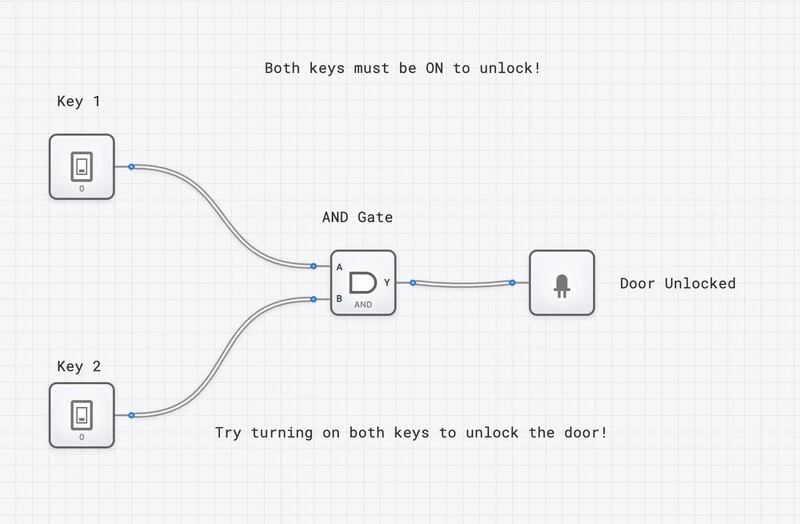
A two-key safe deposit box captures the idea: one key is not enough, the other key is not enough, the door opens only when both keys are turned simultaneously. That principle of unanimous consent is the AND gate.
The Definition: A Gate of Unanimity
An AND gate is a basic digital logic gate that produces a HIGH output (represented as a ‘1’) only when all of its inputs are simultaneously HIGH. If any input is LOW (a ‘0’), the output will be LOW.
In the hierarchy of digital systems, the AND gate sits at the very bottom of the “Combinational Logic” layer. It doesn’t remember the past—it doesn’t have memory like a D_FLIP_FLOP—it simply reacts to the present state of its inputs. This “all-or-nothing” behavior makes it the fundamental tool for creating logical conditions. If you need a circuit to ask, “Are conditions A and B and C all true?”—you need an AND gate.
In digisim.io, the AND component provides a clean representation of this logic. When you’re first starting out, examine the component in isolation before embedding it inside a complex CPU architecture.
The Truth Table: Logic in Black and White
The behavior of any logic gate is exhaustively described by its truth table. For a standard 2-input AND gate, the relationship between its inputs (A and B) and its output (Y) is simple and absolute.
| Input A | Input B | Output Y |
|---|---|---|
| 0 | 0 | 0 |
| 0 | 1 | 0 |
| 1 | 0 | 0 |
| 1 | 1 | 1 |
Notice the pattern: three out of the four possible states result in a ‘0’. Only the final case, where A and B are both ‘1’, “unlocks” the gate and allows a ‘1’ to pass to the output. This strict requirement is what makes the AND gate so powerful for control and validation. If you’re designing a safety system for a heavy industrial press, you might use an AND gate to ensure the machine only fires if the “Start” button is pressed and the safety shield is closed.
The Boolean Logic: Expressing Agreement Mathematically
In the language of Boolean algebra, the AND operation is represented by a dot (), which functions remarkably like standard multiplication. The equation for a 2-input AND gate is:
Often, for simplicity, the dot is omitted, just as in standard algebra:
This mathematical notation perfectly captures the gate’s function. If A is 1 and B is 1, then . However, if either A or B is 0, the entire expression evaluates to 0, precisely mirroring the truth table: and .
When we move into more complex designs, like arithmetic circuits and ALU construction, you’ll see the AND gate performing the “carry” logic in a HALF_ADDER. In that context, the Boolean expression becomes , because a carry only occurs when both bits being added are 1. For more on the broader gate family, see Logic Gate Truth Tables.
Common Pitfall: The Illusion of Instantaneous Logic
Here is where most students run into trouble. In early sketches, it is easy to assume that logic gates operate instantly. You flip an INPUT_SWITCH, and the output changes at the exact same moment.
In the physical world—and in high-fidelity simulations like digisim.io—this is a convenient fiction. Every gate suffers from propagation delay ().
Propagation delay is the tiny, yet finite, amount of time it takes for the output of a gate to respond to a change in its inputs. It’s caused by the physical reality of electrons moving through transistors and the time required to charge or discharge parasitic capacitance.
Why does this matter?
In a simple circuit with one gate, is negligible. But imagine a chain of ten AND gates. If each gate has a delay of 1ns, the final output won’t reflect the input change for 10ns.
If you have two signals arriving at an AND gate from different paths—one through a single gate and another through a complex chain of five gates—they will arrive at different times. This can lead to a “glitch” or a “hazard,” where the AND gate briefly outputs a ‘0’ or ‘1’ that shouldn’t be there.
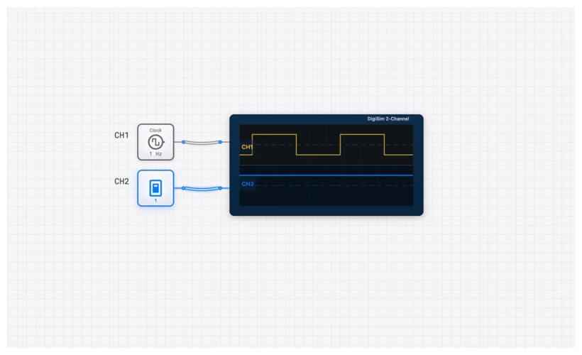
When debugging circuits in digisim.io, use the OSCILLOSCOPE. By connecting one channel to your input and another to the output of the AND gate, you can actually visualize this timing relationship.
Simulating on digisim.io: A Practical Walkthrough
Theory is one thing; seeing the signal propagate is another. Let’s build a basic verification circuit.
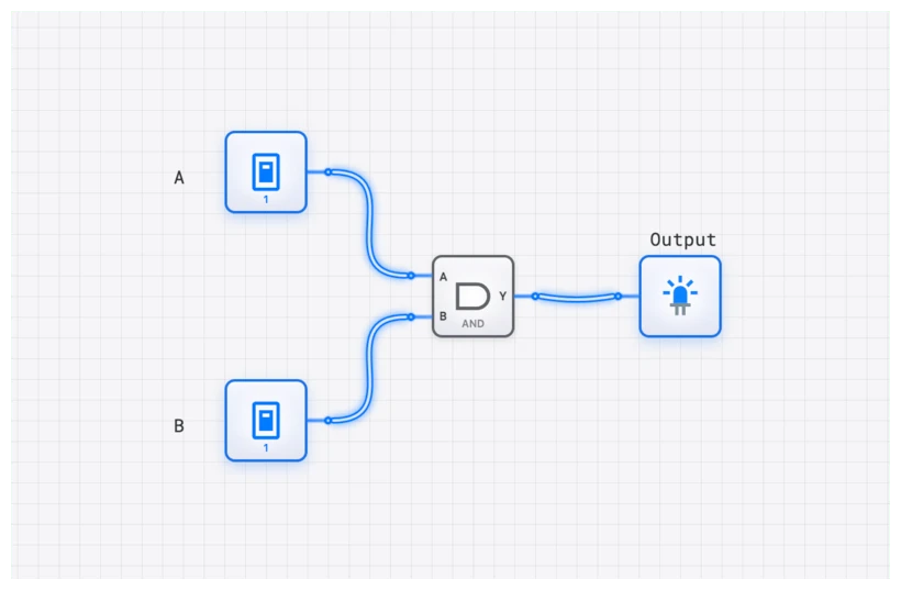
- Place the Inputs: Drag two INPUT_SWITCH components onto the canvas. Label them “Sensor_A” and “Sensor_B”.
- Add the Logic: Place a standard AND gate.
- Add the Output: Place an OUTPUT_LIGHT.
- Wiring: Connect the switches to the inputs and the gate output to the light.
Once wired, use the SimCast feature to record your interaction. Toggle Sensor_A. Nothing happens to the light. Toggle Sensor_B while Sensor_A is off. Still nothing. Only when you toggle both to the ‘1’ state does the signal path turn green (indicating a HIGH state) and the light illuminate.
But let’s take it a step further. To truly understand the “gatekeeper” nature of the AND gate, let’s look at a real-world application: a security system.
In this template, the AND gate acts as the final decision-maker. It requires both an “Armed” signal and a “Motion Detected” signal to trigger the alarm. If the system isn’t armed, the motion sensor can trip all day, but the AND gate will block that signal from reaching the siren.
Real-World Use Case 1: Bit Masking in Processors
The AND gate’s role as a logical “filter” makes it indispensable in modern computing, specifically in an operation called Bit Masking.
Imagine you are writing firmware for a microcontroller and you receive an 8-bit status byte from a sensor. However, you only care about the lowest 4 bits. How do you “erase” the top 4 bits without changing the ones you need? You use an AND operation with a “mask.”
Let’s look at the math:
- Data:
- Mask:
When we perform a bitwise AND:
Because and , the ‘0’s in our mask effectively “blocked” the bits we didn’t want, while the ‘1’s allowed the bits we did want to pass through unchanged. This happens millions of times per second inside the ALU_8BIT of your computer’s processor.
Real-World Use Case 2: Clock Gating for Power Management
If you have ever wondered how your smartphone manages to last a full day despite having a powerful processor, the answer is often “Clock Gating”—powered by the AND gate.
In a synchronous digital system, the CLOCK signal toggles constantly, causing transistors to switch and consume power. But what if a specific part of the chip (like the floating-point unit) isn’t being used?
Designers place an AND gate in the path of the clock signal. One input is the master CLOCK, and the other is an “Enable” signal from the CONTROL_UNIT.
- Enable = 1: The clock pulses pass through the AND gate (). The unit runs.
- Enable = 0: The output of the AND gate stays at 0 (). The clock “stops” for that unit, and power consumption drops to near zero.
This is a cornerstone of “Green Computing.” By simply adding an AND gate, we can turn off entire sections of a CPU when they aren’t needed.
Connecting to the Curriculum
The AND gate sits at the foundation of every other topic on the site:
- Digital Logic 101 covers the basic gates (AND, OR, NOT).
- De Morgan’s Laws shows how to create an AND gate using only NAND gates.
- The Half Adder shows how AND gates form the basis of arithmetic.
Final Thoughts from the Lab
The AND gate is simple, but its role is foundational. Whether you’re masking bits in an ALU_8BIT or gating a clock for power efficiency, you are using the principle of unanimity.
A productive next step is to build a 3-input AND gate using only 2-input AND components — the construction is just . Then continue to the OR gate to compare unanimous-consent logic with democratic-vote logic.
Open the AND component or build your own circuit to verify the truth table.