The Humble NOT Gate: Inversion's Power in Digital Logic
The NOT gate inverts its single input: 0 becomes 1, 1 becomes 0. From ring oscillators to active-low signaling, inversion is the operation logic needs.

TL;DR: The NOT gate (inverter) takes a single input and outputs its logical complement: . It is the third member of the AND/OR/NOT functionally complete set. Beyond simple inversion, NOT gates are the active element in ring oscillators (odd number of inverters in a loop) and the basis for universal NAND/NOR constructions.
The NOT gate is the simplest combinational element on the chip — one input, one output, no shared logic. But inversion is the operation that turns AND into NAND, OR into NOR, and lets a clock signal generate itself in a ring oscillator. Without it, the AND-OR-NOT functionally complete set collapses to two gates that cannot represent every Boolean function.
The Definition: An Act of Logical Opposition
The NOT gate, formally known as an inverter, is a digital logic gate with a single input and a single output. Its function is elegantly simple: it outputs the logical opposite, or complement, of its input.
In the binary world of 0s and 1s, there is no middle ground. If the input is HIGH (logic 1), the output is LOW (logic 0). If the input is LOW (logic 0), the output is HIGH (logic 1). This act of “flipping the bit” is the most fundamental operation in digital electronics.
In circuit diagrams, you’ll recognize the NOT gate as a triangle pointing in the direction of signal flow, capped with a small circle. That circle—often called an “inversion bubble”—is the most important part of the symbol. In digital design, whenever you see that bubble on an input or output of any component, it means an inversion is happening.
Technical Specification: The Truth Table
The behavior of a NOT gate is perfectly described by the simplest truth table in existence. Since there is only one input, we only have two possible states to account for.
| Input (A) | Output (Y) |
|---|---|
| 0 | 1 |
| 1 | 0 |
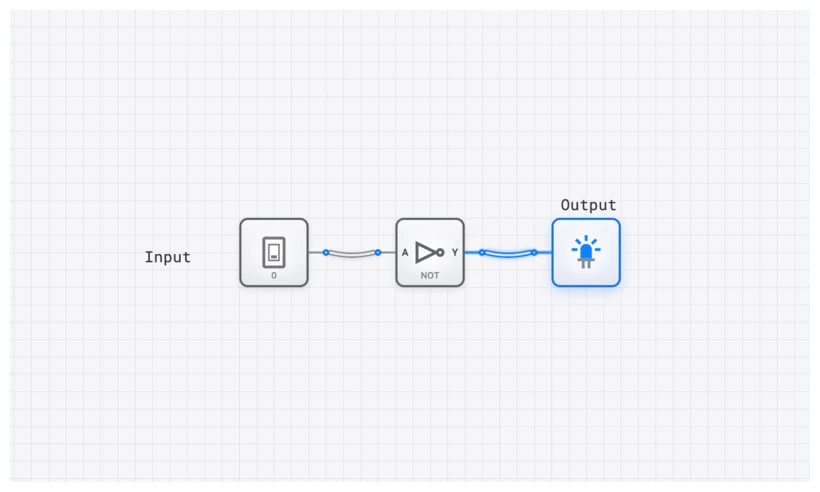
This table is the bedrock of its function. On digisim.io, you can verify this in seconds by connecting an INPUT_SWITCH to a NOT gate and observing the output on an OUTPUT_LIGHT.
The Boolean Logic: Expressing Negation
In the language of Boolean algebra, inversion is represented by an overbar (vinculum), a prime symbol, or a negation symbol. If the input is and the output is , the function of a NOT gate is expressed as:
You will also frequently see this written as or . All these notations mean the same thing: is NOT .
One of the first “aha!” moments in studying digital logic is the Law of Double Negation. If you pass a signal through two NOT gates in series, what happens? The first gate flips it, and the second gate flips it back.
While this might seem redundant, it’s a technique we use constantly in real-world engineering to “buffer” a signal—strengthening it so it can drive more components without losing its logical value—or to introduce a very specific amount of delay.
Common Pitfall: Inversion Isn’t Instantaneous
Here is where many students trip up. In a textbook, a NOT gate is an abstract mathematical concept. In a real circuit, it’s a physical device made of transistors. Because of this, it is subject to the laws of physics, specifically propagation delay.
Propagation delay () is the tiny, finite amount of time it takes for a change at the input to be reflected at the output. It’s the gate’s “reaction time.” While we often measure this in nanoseconds (ns) on the digisim.io simulator, in a modern Intel or AMD processor, this happens in picoseconds.
Why should you care? Because timing is everything.
- Race Conditions: In a complex circuit, if one signal travels through three gates and another travels through only one, they will arrive at their destination at different times. This can cause “glitches” where the output flickers to an incorrect state for a fraction of a second.
- Clock Speed: The maximum speed of a CPU is limited by the longest path a signal has to take through these gates. If the propagation delays add up to more than one clock cycle, the computer fails.
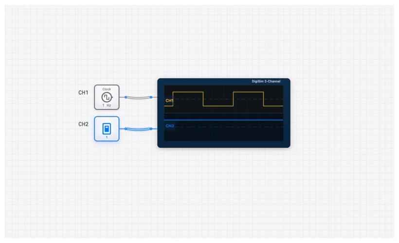
When designing in digisim.io, use the OSCILLOSCOPE to watch these transitions. The output doesn’t change at the exact same moment as the input — that gap is the reality of hardware design. For deeper coverage, see Propagation Delay: The Physics That Dictates Digital Speed.
Simulating the NOT Gate on digisim.io
To truly understand the NOT gate, see it struggle against time. The following workflow makes the timing visible:
- Basic Verification: Place an INPUT_SWITCH, a NOT gate, and an OUTPUT_LIGHT. Toggle the switch. Notice the light is on when the switch is off. Simple, right?
- The Buffer Chain: Place six NOT gates in a row. Connect the output of one to the input of the next. Connect the final output to an OUTPUT_LIGHT. Does the light match the switch? (Hint: count the inversions).
- Timing Analysis: Connect an OSCILLOSCOPE to the input of your first gate and another channel to the output of the last gate. Toggle the switch and look at the waveforms. You’ll see the phase shift caused by the cumulative propagation delay.
Build Your First Inverter Circuit
Real-World Applications: The Heartbeat and the Universe
The NOT gate’s simplicity belies its versatility. It isn’t just a “helper” gate; it’s a foundational requirement for two of the most important concepts in computing.
1. The Ring Oscillator (The Heartbeat)
How do you create a clock signal—the steady “tick-tock” that tells a CPU when to move to the next instruction—without an external crystal? You use an odd number of NOT gates connected in a circle.
Imagine three NOT gates wired in a loop. The output of the third feeds back into the input of the first.
- Suppose the first gate’s input is 0. Its output is 1.
- That 1 propagates to the second gate, which outputs 0.
- That 0 propagates to the third gate, which outputs 1.
- That 1 feeds back to the first gate’s input, forcing its output to flip to 0.
- The new 0 propagates through the second gate (output becomes 1), then the third (output becomes 0), which feeds back again.
The signal “chases its tail” indefinitely, producing a continuous square wave. The frequency of this oscillation is governed entirely by the cumulative propagation delay of the three gates: . This is how many on-chip oscillators generate their own timing signals without an external crystal.
To build this on digisim.io, place three NOT gates in a chain and connect the output of the last gate back to the input of the first. Attach an OSCILLOSCOPE to the output of any gate in the ring. You will see a steady oscillating waveform whose period reveals the total propagation delay of the loop.
2. Universal Logic (NAND and NOR)
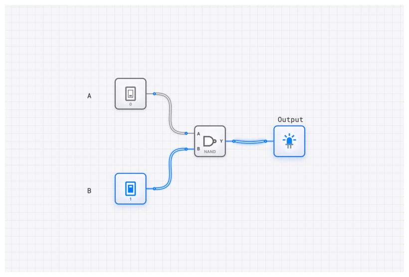
In the early days of computing, engineers realized that manufacturing dozens of different types of gates was expensive. They discovered “Universal Gates.” A NAND gate (which is just an AND gate followed by a NOT gate) can be used to build any other logic gate.
You can build an OR gate using only NAND gates. You can build an XOR gate using only NAND gates. But you can’t do any of that without the inversion property provided by the NOT function. (Aside: “NAND Flash” in your SSD is named for an unrelated reason — its memory cells are wired in series like the pull-down network of a NAND logic gate — but the universality of NAND is what makes it the dominant logic primitive in CMOS standard-cell libraries.)
Explore Universal Logic Templates
Related Topics in the Curriculum
These related posts deepen the picture:
- Digital Logic 101 — AND, OR, NOT in context.
- De Morgan’s Laws — how NOT transforms AND ↔ OR.
- The Clock Pulse — using inversion in ring oscillators for timing.
Final Thoughts
The ability to invert a signal is what allows comparison, memory, and synchronization. When debugging in digisim.io, check logic polarity first. Forgotten inverter? Active-low signal where active-high was expected?
Try building a 3-stage ring oscillator. Use the OSCILLOSCOPE to measure the frequency, then continue to The NAND Gate to see how inversion combines with AND to produce a universal gate. Open the NOT component reference for the truth table.