Mastering Sequential Logic: The D Latch Explained and Simulated
The D latch fixes the SR latch's forbidden state by tying Set and Reset to one Data input gated by Enable. Derive the characteristic equation here.

TL;DR: A D latch stores one bit. It has two inputs (Data and Enable) and follows the characteristic equation . When Enable is HIGH, the latch is transparent — Q follows D. When Enable is LOW, Q holds its last value. The D latch fixes the SR latch’s forbidden state by construction.
Sequential logic — the art of building circuits with memory — typically starts with the SR latch. The SR latch carries a critical flaw: the “forbidden” state where both Set and Reset are active simultaneously, which leaves the output indeterminate. The D_LATCH (Data Latch) fixes this with a single inverter, making it one of the most important building blocks in sequential design.
Deconstructing the D_LATCH: What It Is and Why It Matters
At its core, a D_LATCH is a memory element designed to solve the ambiguity of the SR_LATCH. It does this by ensuring the Set and Reset conditions can never be met at the same time. In the hierarchy of digital systems, the D_LATCH sits right between basic combinational gates and the more complex D_FLIP_FLOP. While gates respond only to current inputs, the D_LATCH remembers.
The component features two primary inputs and two outputs:
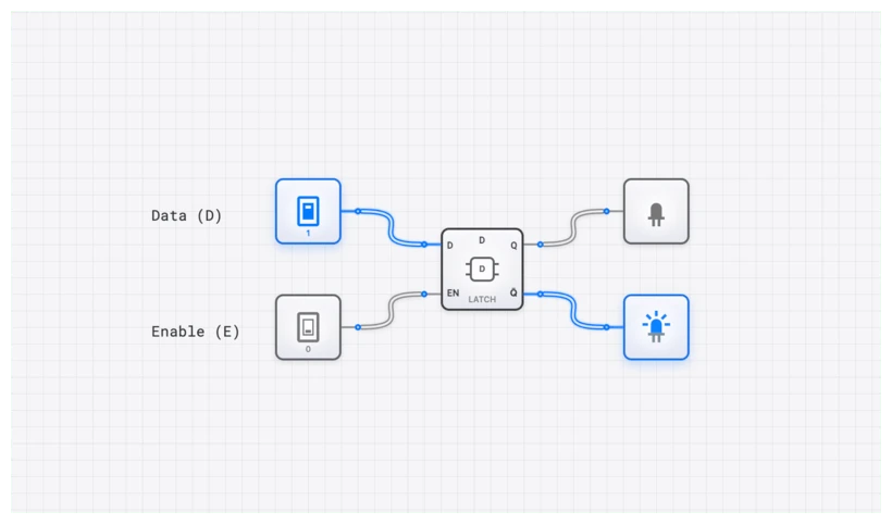
- D (Data): A single input that determines what value (0 or 1) the latch should store.
- E (Enable): Often labeled ‘E’ or ‘G’ (Gate), this input acts as a control switch. It dictates when the latch pays attention to the D input.
- Q: The primary output, which reflects the stored data.
- : The complemented (inverted) output of the stored data.
The behavior is defined by two distinct modes of operation based on the state of the Enable signal. When , the latch is in Transparent Mode. The output Q simply follows the state of the D input. If D changes, Q changes with it almost instantaneously. When , the latch enters Latched Mode. The Q output ignores the D input completely and holds onto the last value it had just before E transitioned from 1 to 0.
Technical Specification and Truth Table
To master the D_LATCH, you have to look past the symbol and understand the logic governing its state transitions. The truth table clearly defines the next state of Q () based on the current inputs. Note that when E is 0, the D input is irrelevant, denoted by an ‘X’ for “Don’t Care.”
| E (Enable) | D (Data) | Action | |
|---|---|---|---|
| 0 | X | Hold (Latched) | |
| 1 | 0 | 0 | Reset (Transparent) |
| 1 | 1 | 1 | Set (Transparent) |
The Characteristic Equation
We can express this behavior mathematically with the D_LATCH characteristic equation. This equation is the formal definition of the circuit’s operation and is essential for Boolean simplification in larger sequential designs.
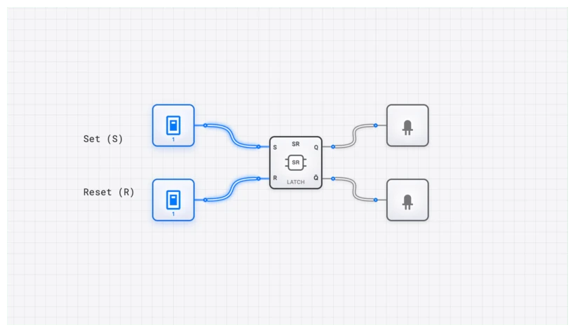
Let’s derive this from first principles. The D_LATCH is internally a gated SR Latch where:
The SR Latch characteristic equation states . Substituting:
Applying De Morgan’s Law: . So:
Since already covers the case where both D and Q are relevant, the term is absorbed by Boolean simplification (consensus theorem), leaving us with the clean result:
Breaking this into its logical components:
- The term represents the transparency: if Enable is high, the output becomes whatever D is.
- The term represents the memory: if Enable is low, the output maintains its current state .
- The equation is a multiplexer in disguise: the Enable signal selects between new data and the stored value.
The Logic Under the Hood: From SR to D
You can think of the D_LATCH as a “Gated SR_LATCH” with a clever twist. If you look at the internal gate structure, we feed the D input directly to the “Set” side and an inverted D input (via a NOT gate) to the “Reset” side. This guarantees that S and R are always opposites when the circuit is enabled.
When , if , then and (Set). If , then and (Reset). The forbidden state is now physically impossible to reach through the D input. When , both and are forced to 0, causing the underlying SR_LATCH structure to hold its value.
Common Pitfall: The Peril of Transparency
The D_LATCH’s greatest strength—its transparency—is also its most significant weakness in complex, high-speed systems. This is the critical pitfall that trips up many students when they move from simple circuits to CPU design.
Because the output Q follows the input D for the entire duration that the Enable signal is high, any noise, glitches, or unintended signal changes on the D line will pass directly to the output. This is known as level-sensitive behavior.
Imagine the Enable signal is a window. When , the window is wide open. You see everything happening outside (the D input) in real-time, including a bird flying by or a leaf falling (the “glitches”). When , the window is instantly frosted over, displaying a snapshot of the very last thing you saw.
Why transparency is dangerous in practice: Consider a system where the output of one D_LATCH feeds through combinational logic and back into the input of the same or another latch. While the Enable is high, any change at the output immediately propagates through the logic and appears at the input, which then changes the output again. This creates a feedback path through the combinational logic that can cause:
- Unintended multiple state changes within a single enable window.
- Glitch propagation, where a transient spike on the data line passes through to Q and corrupts downstream circuits.
- Timing unpredictability, where the final value latched depends on when exactly the Enable falls—a nightmare for verification.
This is precisely why synchronous designs ultimately prefer the D flip-flop, which narrows the “window” to the vanishingly small moment of a clock edge. But before you can master the edge, you must master the level. Understanding transparency is what makes the flip-flop’s edge-triggering solution feel elegant rather than arbitrary.
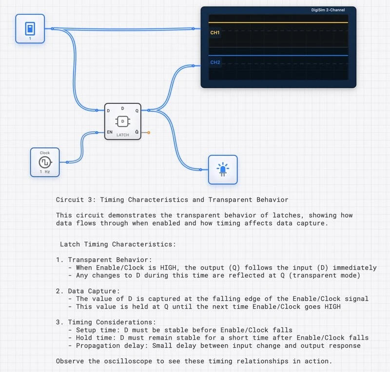
Oscilloscope Verification: Seeing the Signal
To truly understand the timing of a D_LATCH, you need to see the waveforms. In digisim.io, the OSCILLOSCOPE is your best friend for debugging these timing relationships.
When you connect an OSCILLOSCOPE to the E, D, and Q pins, you’ll notice a few critical behaviors:
- Propagation Delay (): There is a tiny gap between D changing and Q changing during the transparent phase. This is the time it takes for electrons to flow through the internal AND and NOR gates.
- The Latching Moment: Watch the Q line exactly when E drops from 1 to 0. Whatever value D had at that precise microsecond is what Q will hold, regardless of what D does afterward.
- Glitch Capture: If you toggle D rapidly while E is high, you’ll see those pulses mirrored on Q. If you toggle D while E is low, the Q line on the OSCILLOSCOPE remains a flat, steady horizontal line.
Real-World Applications: Beyond the Breadboard
The D_LATCH isn’t just an academic exercise; it’s a workhorse component found in the architecture of the devices you use every day.
1. CPU Pipeline Registers
In a modern pipelined processor, an instruction goes through multiple stages: Fetch, Decode, Execute, and Write-back. Between each stage, a bank of latches (often grouped into a REGISTER) forms a pipeline register. They capture the output of one stage and hold it steady so the next stage has a stable input to work with. This allows the CPU to work on different parts of multiple instructions simultaneously, dramatically increasing throughput.
2. Address Demultiplexing (The Intel 8086 Example)
To save physical pins on integrated circuits, early microprocessors like the Intel 8085 and 8086 used a multiplexed address/data bus. For part of a machine cycle, the pins would carry a memory address; for another part, they would carry data.
Engineers used an external D_LATCH (like the famous 74LS373 Octal Transparent Latch) to “demultiplex” these signals. The processor would place the address on the bus and pulse a signal called ALE (Address Latch Enable). The D_LATCH would grab the address and hold it for the memory chips, freeing the processor’s pins to then send or receive data. Without the D_LATCH, we would have needed twice as many pins on the CPU, making it larger and much more expensive.
Building the D_LATCH on digisim.io
Theory is essential, but intuition comes from wiring it up. The build below uses two AND gates, two NOR gates, and a NOT gate.
Step-by-Step Construction
- Place the Gates: Drag two AND gates, two NOR gates, and one NOT gate onto the canvas.
- Setup Inputs: Add two INPUT_SWITCH components. Label one “Data” and the other “Enable”.
- The Input Logic:
- Connect “Data” to the top AND gate.
- Connect “Data” to the NOT gate, then connect the NOT output to the bottom AND gate.
- Connect “Enable” to the second input of both AND gates.
- The Memory Core:
- Connect the output of the top AND gate to the input of a NOR gate.
- Connect the output of the bottom AND gate to the input of the second NOR gate.
- The Cross-Couple: This is the magic part. Connect the output of the top NOR gate to the input of the bottom NOR gate. Connect the output of the bottom NOR gate back to the input of the top NOR gate.
- Output: Connect an OUTPUT_LIGHT to the output of the bottom NOR gate. This is your Q.
The SimCast Experience
The SimCast feature in digisim.io plays signal propagation in slow motion. Watch the “Enable” signal act as a gatekeeper: a HIGH on Data reaches the input AND gates but stops there until Enable also goes HIGH.
Related Topics in the Curriculum
As you continue exploring digital logic on digisim.io, these related topics will deepen your understanding:
The D_LATCH is a pivotal point in our structured learning path on digisim.io. It marks the transition from “what is happening now” to “what happened before.”
- The SR latch — the foundation and the forbidden state problem.
- The D_LATCH (this article) — level-sensitive memory.
- The D flip-flop — moving from level-sensitivity to edge-triggering.
- The 4-bit register — combining flip-flops to store a multi-bit word.
- Setup, hold, and metastability — the timing constraints behind every latched circuit.
Final Thoughts: The First Step to Memory
The D_LATCH is the first real step toward understanding how a computer stores state. It fixes the instability of the SR_LATCH and introduces enabled data capture. Edge-triggered flip-flops handle most synchronous designs, but the D_LATCH remains the fundamental cell of transparent memory.
Continue with the D flip-flop to see how edge-triggering closes the transparency window, or open the D_LATCH component reference.