8-bit Adder
Overview
- Purpose: The 8-bit Adder is a digital circuit that performs binary addition on two 8-bit numbers. It accepts two 8-bit inputs (A and B), along with an optional carry-in bit (Cin), and produces an 8-bit sum output (S) and a carry-out bit (Cout).
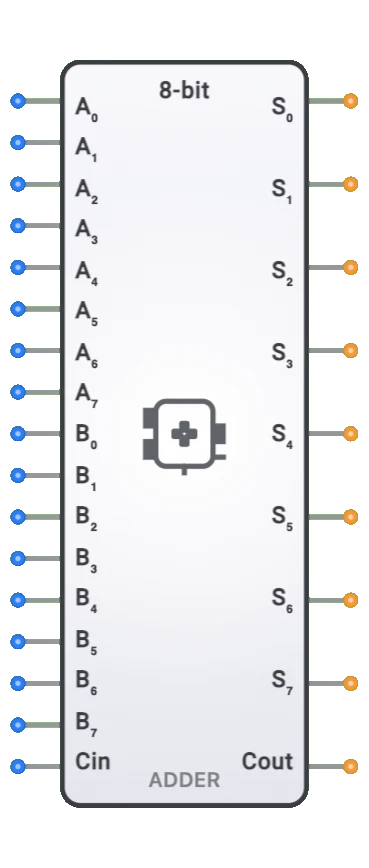
- Symbol: The 8-bit Adder is represented by a rectangular block with inputs for the two 8-bit operands (A[7:0] and B[7:0]) and carry-in (Cin) on the left side, and outputs for the 8-bit sum (S[7:0]) and carry-out (Cout) on the right side.
- DigiSim.io Role: Serves as a fundamental building block in arithmetic logic units (ALUs), forming the basis for implementing various arithmetic operations in digital systems including processors, calculators, and control units.
Functional Description
Logic Behavior
The 8-bit Adder performs binary addition according to the equation: A + B + Cin = (Cout, S). Each bit position adds the corresponding bits from A and B along with the carry from the previous position.
Truth Table (Sample Entries - Due to 2^17 possible combinations):
| A[7:0] | B[7:0] | Cin | S[7:0] | Cout | Note |
|---|---|---|---|---|---|
| 00000000 (0) | 00000000 (0) | 0 | 00000000 (0) | 0 | Zero addition |
| 00000001 (1) | 00000001 (1) | 0 | 00000010 (2) | 0 | Simple addition |
| 11111111 (255) | 00000001 (1) | 0 | 00000000 (0) | 1 | Overflow to 256 |
| 10101010 (170) | 01010101 (85) | 0 | 11111111 (255) | 0 | Complementary inputs |
| 11111111 (255) | 11111111 (255) | 0 | 11111110 (254) | 1 | Maximum + maximum |
Inputs and Outputs
Inputs:
- A[7:0]: 8-bit first operand.
- B[7:0]: 8-bit second operand.
- Cin: 1-bit carry input for cascading with other adders or for incrementation.
Outputs:
- S[7:0]: 8-bit sum result.
- Cout: 1-bit carry output indicating overflow beyond 8 bits.
Configurable Parameters
- Propagation Delay: The time it takes for outputs to change after input changes, configurable in DigiSim.io simulation settings.
- Implementation Method: Some versions may allow selection between different internal implementations (ripple carry, carry lookahead, etc.) affecting speed and resource usage.
Visual Representation in DigiSim.io
The 8-bit Adder is displayed as a rectangular block with clearly labeled inputs on the left side (A[7:0], B[7:0], Cin) and outputs on the right side (S[7:0], Cout). When connected in a circuit, the component visually indicates the current values on its inputs and outputs through the color coding of wires, allowing users to track the flow of binary data through the system.
Educational Value
Key Concepts
- Binary Addition: Demonstrates how computers perform addition on binary numbers.
- Carry Propagation: Illustrates how carries flow from less significant to more significant bits.
- Digital Arithmetic: Shows the fundamental building block for computer arithmetic operations.
- Overflow Detection: Introduces the concept of detecting when a result exceeds the available bit width.
- Modular Design: Exemplifies how complex operations can be built from simpler components.
Learning Objectives
- Understand binary addition and how it's implemented in digital circuits.
- Learn how carry propagation affects the performance of digital adders.
- Recognize different adder implementations and their trade-offs.
- Apply 8-bit adders in designing arithmetic circuits and simple processors.
- Comprehend how overflow is detected and handled in fixed-width arithmetic.
Usage Examples/Scenarios
- Arithmetic Logic Units (ALUs): Core component for CPU arithmetic operations and address calculations.
- Binary Counters: Creating synchronous counters with specific counting sequences.
- Digital Signal Processing: Sample value calculations and signal amplitude operations.
- Memory Address Generation: Calculating offsets and addresses in memory systems.
- Multiplication Circuits: Building block for implementing multiplication via repeated addition.
- Program Counter: Incrementing the program counter in a CPU design.
Technical Notes
- The 8-bit adder can be implemented using various architectures that trade off between speed and complexity:
- Ripple Carry Adder: Simplest implementation but has linear delay with bit width.
- Carry Lookahead Adder: Faster operation with logarithmic delay but more complex circuitry.
- Carry Select Adder: Good compromise between speed and resources.
- For signed arithmetic, the carry-out does not correctly indicate overflow; instead, overflow occurs when the sign of the result differs unexpectedly from the operands.
- Multiple 8-bit adders can be cascaded to perform addition on wider data (16-bit, 32-bit, etc.) by connecting the carry-out of one adder to the carry-in of the next.
- In DigiSim.io, the adder's propagation delay simulates real-world behavior, with the worst-case delay occurring when a carry must propagate from the least significant bit to the most significant bit.
Characteristics
Input Configuration:
- Two 8-bit binary inputs (A[7:0] and B[7:0])
- One carry-in bit (Cin) for cascading with other adders
- Standard digital logic levels for all inputs
- Typically features high input impedance
Output Configuration:
- 8-bit sum output (SUM[7:0])
- One carry-out bit (Cout) indicating overflow
- Compatible with standard digital logic levels
- Can drive standard digital loads
Functionality:
- Performs binary addition: SUM = A + B + Cin
- Generates carry-out when result exceeds 8 bits
- Numerically adds unsigned binary values from 0 to 255
- Can be used for signed arithmetic with appropriate interpretation
- Achieves efficient arithmetic operations in digital systems
Propagation Delay:
- Total delay: 20-50ns (technology dependent)
- Worst-case path: from least significant bit to carry-out
- Critical path: through carry chain (ripple carry design)
- Reduced in optimized designs (carry lookahead, etc.)
- Temperature and load dependent
Fan-Out:
- Typically drives 10-20 standard loads
- May require buffering for high fan-out applications
- Output loading affects propagation delay
Power Consumption:
- Static: Low to moderate depending on technology
- Dynamic: Proportional to switching frequency
- Increases with higher data switching rates
- Power efficient in CMOS implementations
- Higher in ripple carry compared to some advanced designs
Circuit Complexity:
- Moderate (8 full adders plus interconnections)
- Higher complexity in carry lookahead implementations
- Implementation complexity varies with design approach
- Increases with performance optimization techniques
Implementation Methods
Ripple Carry Adder
- Chain of 8 full adders connected sequentially
- Carry output of each stage feeds into next stage's carry input
- Simplest implementation method
- Lower component count but higher propagation delay
- Delay increases linearly with operand width
- Example chip: 74283 (4-bit adder, two needed for 8 bits)
Carry Lookahead Adder
- Calculates carry signals in advance based on generate/propagate logic
- Significantly reduced delay compared to ripple carry
- Higher component count but much faster operation
- More complex circuitry for carry prediction
- Better for high-speed applications
- Implementation may use 74182 look-ahead generator
Carry Select Adder
- Calculates results for both possible carry input values
- Multiplexers select the correct result when carry is known
- Compromise between speed and circuit complexity
- Partial parallel operation reduces delay
- Effective for medium to high-performance applications
Carry Skip Adder
- Groups of bits checked to determine if carries can "skip" ahead
- Faster than ripple carry but simpler than lookahead
- Good balance of complexity versus speed improvement
- Optimized for average-case performance
Integrated Circuit Implementation
- Dedicated 8-bit adder ICs
- Standard logic families (TTL, CMOS, etc.)
- Often include features like carry enable/disable
- Examples: 74283 (4-bit) cascaded, 74HC283, custom ICs
- May include additional functionality (flags, overflow detection)
FPGA/ASIC Implementation
- Implemented in programmable logic or custom silicon
- Can be optimized for speed, area, or power consumption
- Often includes dedicated hardware for fast carry propagation
- Highly configurable for specific applications
- Available as IP cores in design libraries
Applications
Binary Arithmetic Operations
- Direct binary addition
- Subtraction (using two's complement and adders)
- Base for multiplication and division circuits
- Binary coded decimal (BCD) addition
- Incrementing/decrementing counters and pointers
Arithmetic Logic Units (ALUs)
- Core component in CPU arithmetic sections
- Used in program counter and address calculations
- Data path operations in processors
- Floating-point arithmetic (as component)
- Mathematical coprocessors
Digital Signal Processing
- Sample processing in digital filters
- FFT implementations
- Signal generation and analysis
- Digital audio/video processing
- Coefficient calculations
Memory Address Calculation
- Offset address computation
- Array indexing
- Stack pointer manipulation
- Page address calculations
- Memory management operations
Data Processing Systems
- Checksum calculation
- Error detection and correction
- Data encryption algorithms
- Hash function computation
- CRC calculations
Control Systems
- Feedback loop calculations
- Position and velocity computations
- PID controller implementations
- State machine transitions
- Sensor data integration
Graphics Processing
- Coordinate calculations
- Pixel address generation
- Color value manipulation
- Texture mapping calculations
- Vector graphics operations
Limitations
Propagation Delay
- Carry propagation bottleneck in ripple carry designs
- Performance decreases with increased bit width
- May limit system clock frequency in critical paths
- Timing considerations critical for synchronous systems
- Requires careful handling in high-speed designs
Overflow Detection
- Simple carry-out only indicates unsigned overflow
- Signed arithmetic requires additional overflow detection
- Extra logic needed for proper overflow handling
- Can be complex to interpret in mixed arithmetic operations
- May require additional circuitry for full ALU functionality
Limited Operations
- Performs only addition natively
- Subtraction requires complementing and carry manipulation
- Complex operations need additional circuitry
- Special cases (like zero detection) may need extra logic
- Limited to fixed-width operands and results
Power and Area Considerations
- Higher performance implementations consume more power
- Carry lookahead adders require more chip area
- Power consumption increases with switching frequency
- Design tradeoffs between speed, area, and power
- Implementation technology affects all aspects of performance
Error Propagation
- Single bit errors propagate through carry chain
- No inherent error detection capability
- May require additional error detection circuits
- Reliability concerns in critical applications
- Fault tolerance requires redundancy or parity checking
Circuit Implementation Detail
Ripple Carry Implementation
graph LR
    A0[A0] --> FA0[Full Adder 0]
    B0[B0] --> FA0
    CIN[Carry In] --> FA0
    FA0 -->|Sum0| S0[S0]
    FA0 -->|Cout| FA1[Full Adder 1]

    A1[A1] --> FA1
    B1[B1] --> FA1
    FA1 -->|Sum1| S1[S1]
    FA1 -->|Cout| FA2[Full Adder 2]

    A2[A2] --> FA2
    B2[B2] --> FA2
    FA2 -->|Sum2| S2[S2]
    FA2 -->|Cout| FA7[Full Adder 7]

    A7[A7] --> FA7
    B7[B7] --> FA7
    FA7 -->|Sum7| S7[S7]
    FA7 -->|Cout| COUT[Carry Out]
Ripple Carry: Carry propagates sequentially from LSB (FA0) to MSB (FA7).
Example 4-bit Adder IC (74283) - Two needed for 8 bits
Pin Configuration (74283):
| Pin Group | Pins | Function |
|---|---|---|
| A Inputs | A0-A3 | 4-bit input A |
| B Inputs | B0-B3 | 4-bit input B |
| Carry In | Cin | Carry input |
| Sum Outputs | Sum0-Sum3 | 4-bit sum output |
| Carry Out | Cout | Carry output |
| Power | VCC, GND | +5V and Ground |
8-bit Implementation:
- IC1 (LSB): Handles A0-A3, B0-B3 → Sum0-Sum3
- IC2 (MSB): Handles A4-A7, B4-B7 → Sum4-Sum7
- Cascade: IC1.Cout connects to IC2.Cin
Related Components
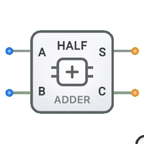
- Half Adder: Simple adder with two inputs and no carry-in
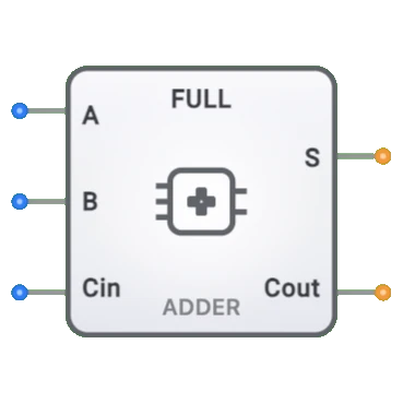
- Full Adder: Basic one-bit adder with carry-in and carry-out
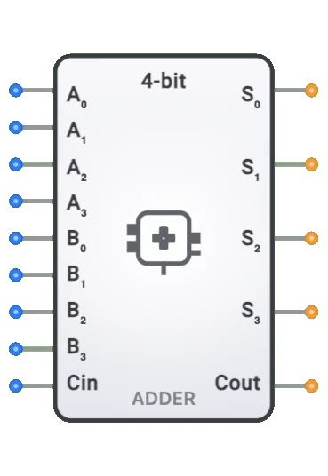
- 4-bit Adder: Smaller version handling 4-bit operands
- 16-bit/32-bit Adder: Larger versions for wider operands
- Binary Counter: Uses adders for incrementing operations
- Arithmetic Logic Unit (ALU): Incorporates adders with other logical functions
- Binary Subtractor: Complement of the adder, often implemented using adders
- BCD Adder: Special adder for decimal calculations using binary coded decimal
- Carry Lookahead Generator: Accelerates carry propagation (e.g., 74182)
- Adder-Subtractor: Combined unit that can perform both addition and subtraction