1-to-4 Demultiplexer
Overview
- Purpose: The 1-to-4 Demultiplexer (DEMUX) is a digital circuit that routes a single input signal to one of four possible output lines based on the values of two selection lines. It functions as a data distributor, directing input data to a selected destination.
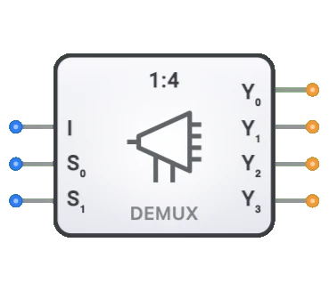
- Symbol: The 1-to-4 Demultiplexer is represented by a rectangular block with one data input (D), two select inputs (S1, S0), and four data outputs (Y0-Y3).
- DigiSim.io Role: Serves as a fundamental data distribution component in digital circuits, enabling selective signal routing to multiple destinations and forming the basis for address decoding and data distribution networks.
Functional Description
Logic Behavior
The 1-to-4 Demultiplexer directs its single input to one of four outputs based on the binary value of the selection inputs. The select inputs act as a 2-bit binary number that determines which output will receive the input value. All other outputs remain at logic 0.
Truth Table:
| S1 | S0 | Y0 | Y1 | Y2 | Y3 | Active Output |
|---|---|---|---|---|---|---|
| 0 | 0 | D | 0 | 0 | 0 | Output 0 |
| 0 | 1 | 0 | D | 0 | 0 | Output 1 |
| 1 | 0 | 0 | 0 | D | 0 | Output 2 |
| 1 | 1 | 0 | 0 | 0 | D | Output 3 |
Note: D is the data input value; only one output is active at a time.
Inputs and Outputs
Inputs:
- D: 1-bit data input that is routed to the selected output.
- S1, S0: Two 1-bit select inputs that determine which output receives the input data.
- Some implementations may include an additional enable input (EN) that can disable all outputs.
Outputs:
- Y0, Y1, Y2, Y3: Four 1-bit data outputs, only one of which is active (equals D) at a time.
Configurable Parameters
- Output Type: Whether the inactive outputs are LOW or high-impedance.
- Enable Control: Some implementations include an enable input that can deactivate all outputs.
- Active Level: Whether the demultiplexer operates with active-high or active-low logic.
- Propagation Delay: The time it takes for the outputs to change after the select inputs change.
Visual Representation in DigiSim.io
The 1-to-4 Demultiplexer is displayed as a rectangular block with labeled inputs on the left side (D, S1, S0) and outputs (Y0, Y1, Y2, Y3) on the right side. When connected in a circuit, the component visually indicates the active data path through color changes on connecting wires, showing which output is currently selected to receive the input value.
Educational Value
Key Concepts
- Signal Distribution: Demonstrates how digital systems selectively route data to multiple destinations.
- Binary Decoding: Illustrates how binary values control signal paths in digital circuits.
- Address Decoding: Shows the fundamental mechanism used in memory and I/O address selection.
- Data Routing: Presents how a single source can be connected to one of several possible destinations.
- Combinational Logic: Reinforces understanding of how logic gates implement data routing functions.
Learning Objectives
- Understand how digital systems distribute signals based on selection controls.
- Learn how binary select values determine which output receives the input data.
- Recognize the inverse relationship between multiplexers and demultiplexers.
- Apply demultiplexer concepts to design address decoders, data distribution networks, and control systems.
- Comprehend how demultiplexers expand limited control signals to multiple endpoints.
Usage Examples/Scenarios
- Address Decoding: Selecting specific memory chips or I/O devices based on address bits.
- Data Distribution: Routing data to one of several possible destinations.
- I/O Port Expansion: Expanding a single output port to control multiple devices.
- Time-Division Demultiplexing: Separating time-multiplexed signals back into individual channels.
- Control Signal Routing: Directing control signals to specific subsystems based on operation codes.
- Display Systems: Selecting individual digits or segments in multiplexed displays.
Technical Notes
- The 1-to-4 demultiplexer can be implemented using basic logic gates (typically 4 AND gates and 2 inverters).
- It can also be constructed by combining a 2-to-4 decoder with AND gates to gate the input data.
- The Boolean expressions for the outputs are:
- Y0 = D · !S1 · !S0
- Y1 = D · !S1 · S0
- Y2 = D · S1 · !S0
- Y3 = D · S1 · S0
- Larger demultiplexers (1-to-8, 1-to-16) can be built by adding more select inputs.
- Demultiplexers and decoders are closely related; a demultiplexer can be viewed as a decoder with an enable input.
- Active-low demultiplexers produce a LOW output on the selected line and HIGH on all others.
- In DigiSim.io, the demultiplexer's behavior simulates real-world digital components with proper handling of select transitions.
Characteristics
- Input Configuration:
- One data input (D)
- Two select inputs (S1, S0) to choose among 4 outputs
- Output Configuration:
- Four outputs (Y0, Y1, Y2, Y3)
- Only one output active at a time
- Propagation Delay:
- Typically 5-15ns (technology dependent)
- Delay from select change to output change
- Delay from data input change to output change
- Power Consumption:
- Low to moderate
- Increases with switching frequency
- Fan-Out:
- Each output typically drives 10-50 gates (technology dependent)
- Logic Levels:
- Compatible with standard logic families (TTL, CMOS)
- Circuit Complexity:
- Medium (requires 4 AND gates and 2 inverters in basic implementation)
- Speed:
- Faster than larger demultiplexers (1-to-8, 1-to-16)
- Suitable for medium-speed applications
- Signal Integrity:
- Maintains signal integrity at outputs
- No signal degradation through the selection path
Implementation Methods
- Using Basic Logic Gates
- Implemented using AND gates and inverters
- Each output is gated with a unique combination of select lines
graph TB
    DataIn[Data Input D] --> AndGate0[AND Gate]
    DataIn --> AndGate1[AND Gate]
    DataIn --> AndGate2[AND Gate]
    DataIn --> AndGate3[AND Gate]

    Select0[S0] --> NotGate0[NOT]
    Select1[S1] --> NotGate1[NOT]

    NotGate0 --> AndGate0
    NotGate1 --> AndGate0

    Select0 --> AndGate1
    NotGate1 --> AndGate1

    NotGate0 --> AndGate2
    Select1 --> AndGate2

    Select0 --> AndGate3
    Select1 --> AndGate3

    AndGate0 --> OutputY0[Y0 Output]
    AndGate1 --> OutputY1[Y1 Output]
    AndGate2 --> OutputY2[Y2 Output]
    AndGate3 --> OutputY3[Y3 Output]
Selection Logic:
- Y0: S1=0, S0=0 (both inverted)
- Y1: S1=0, S0=1
- Y2: S1=1, S0=0
- Y3: S1=1, S0=1
- Using a Decoder with Input Gating
- 2-to-4 decoder generates selection signals
- Each decoder output is ANDed with the data input
graph LR
    S0[S0] --> DEC[2-to-4 Decoder]
    S1[S1] --> DEC

    DEC -->|E0| AND0[AND]
    DEC -->|E1| AND1[AND]
    DEC -->|E2| AND2[AND]
    DEC -->|E3| AND3[AND]

    D[Data D] --> AND0
    D --> AND1
    D --> AND2
    D --> AND3

    AND0 --> Y0[Y0]
    AND1 --> Y1[Y1]
    AND2 --> Y2[Y2]
    AND3 --> Y3[Y3]
Operation: Decoder selects one enable line based on S1:S0, AND gates route data to selected output.
Using Multiplexers in Reverse
- Connecting the data input to all inputs of a multiplexer
- Using the outputs as enable signals for tristate buffers
Integrated Circuits
- Available in 74xx series logic families (e.g., 74139, 74HC139)
- Often provided as dual 1-to-4 demultiplexers in a single package
Applications
Data Distribution
- Routing a single data source to multiple destinations
- Channel selection in communication systems
- Time-division demultiplexing in telecommunications
Memory Systems
- Address decoding for memory chip selection
- Memory bank selection in multi-bank systems
- Register selection in register files
Digital Control Systems
- Control signal distribution
- Command routing in microprocessor systems
- Mode selection in multi-mode devices
I/O Port Expansion
- Expanding limited I/O ports in microcontrollers
- Serial-to-parallel data conversion
- Peripheral device selection
Signal Routing
- Routing clock or control signals to specific subsystems
- Bus control in multi-device systems
- Signal distribution in testing equipment
Decoder Expansion
- Creating larger decoders (e.g., 3-to-8, 4-to-16)
- Memory address decoding in larger memory systems
- Command decoding in complex instruction sets
Display Systems
- Digit selection in multiplexed displays
- Segment routing in LED/LCD display systems
- Pixel addressing in small display matrices
Limitations
Output Activation Limitation
- Only one output active at a time
- Cannot distribute data to multiple outputs simultaneously
Select Line Dependencies
- Select lines must be stable before valid output is available
- Glitches can occur during select line transitions
Propagation Delay
- Signal delay through the demultiplexer can affect timing in high-speed systems
- Delay increases slightly with number of outputs
Fan-out Limitations
- Each output has limited drive capability
- May require buffers for high fan-out applications
Power Consumption
- Increases with switching frequency
- Idle outputs still consume static power in some implementations
Circuit Implementation Detail
Boolean Expressions
The 1-to-4 demultiplexer can be described by the following Boolean expressions:
Y0 = D · !S1 · !S0
Y1 = D · !S1 · S0
Y2 = D · S1 · !S0
Y3 = D · S1 · S0
Where:
- D is the data input
- S1, S0 are the select inputs
- Y0, Y1, Y2, Y3 are the outputs
- "·" represents logical AND
- "!" represents logical NOT
Implementation Analysis
In the gate-level implementation, each output is enabled by a unique combination of the select lines:
- Y0 is active when S1=0 and S0=0
- Y1 is active when S1=0 and S0=1
- Y2 is active when S1=1 and S0=0
- Y3 is active when S1=1 and S0=1
Related Components
- 1-to-2 Demultiplexer: Simpler version with one select line and two outputs
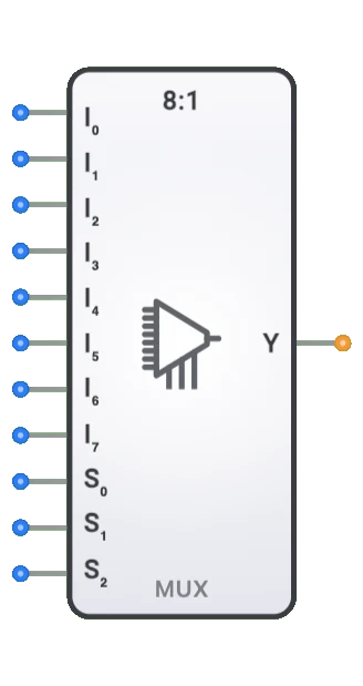
- 1-to-8 Demultiplexer: Extended version with three select lines and eight outputs
- 1-to-16 Demultiplexer: Larger version with four select lines and sixteen outputs
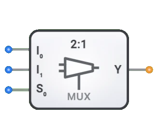
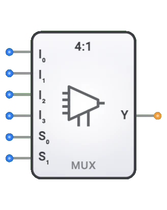
- 4-to-1 Multiplexer: Performs the inverse operation, selecting one of multiple inputs
- 2-to-4 Decoder: Similar component but activates one of multiple outputs based on binary input
- Encoder: Performs the inverse operation of a decoder
- Bus Driver: Often combined with demultiplexers for bus-oriented systems
- Tristate Buffer: Used in demultiplexer implementations for shared bus applications