8-to-1 Multiplexer
Overview
- Purpose: The 8-to-1 Multiplexer is a digital circuit that selects one of eight input signals and forwards it to a single output line, acting as a digitally controlled switch for routing data from multiple sources to a common destination.
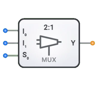
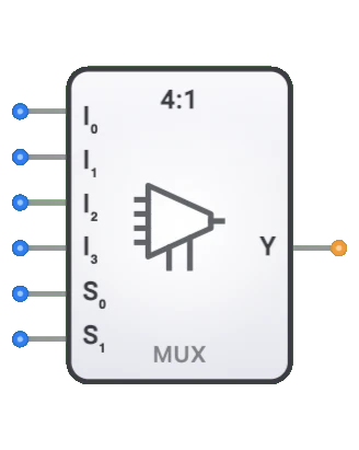
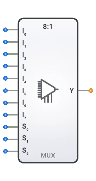
- Symbol: Typically represented as a rectangular block with eight data inputs (D0-D7), three select inputs (S0-S2), and one output (Y).
- DigiSim.io Role: Serves as a fundamental component in digital systems for data selection, path routing, and reducing hardware complexity by enabling multiple data sources to share a common pathway.
Functional Description
Logic Behavior
The 8-to-1 Multiplexer routes one of its eight input signals to the output based on the binary value of the three select lines. The select lines function as a 3-bit address that determines which input channel is connected to the output.
Truth Table:
| S2 | S1 | S0 | Output Y |
|---|---|---|---|
| 0 | 0 | 0 | D0 |
| 0 | 0 | 1 | D1 |
| 0 | 1 | 0 | D2 |
| 0 | 1 | 1 | D3 |
| 1 | 0 | 0 | D4 |
| 1 | 0 | 1 | D5 |
| 1 | 1 | 0 | D6 |
| 1 | 1 | 1 | D7 |
Inputs and Outputs
Inputs:
- D0-D7: Eight 1-bit data inputs, one of which will be routed to the output.
- S0: Least Significant Bit (LSB) of the 3-bit select input.
- S1: Middle bit of the 3-bit select input.
- S2: Most Significant Bit (MSB) of the 3-bit select input.
Outputs:
- Y: Single 1-bit output that reflects the value of the selected input.
Configurable Parameters
- Enable Control: Some implementations include an additional enable input that can disable the output.
- Output Type: Standard, three-state, or open-collector output configurations.
- Active Levels: Whether select inputs and enable signals are active-high or active-low.
- Propagation Delay: The time it takes for the output to reflect changes on the selected input.
Visual Representation in DigiSim.io
The 8-to-1 Multiplexer is displayed as a rectangular block with eight data input pins (D0-D7) and three select input pins (S0-S2) on the left side, and a single output pin (Y) on the right side. When connected in a circuit, the component visually indicates the active data path through color changes on connecting wires.
Educational Value
Key Concepts
- Data Selection: Demonstrates how digital systems choose between multiple data sources.
- Binary Addressing: Shows how binary codes can select specific input channels.
- Signal Routing: Illustrates fundamental concepts of data pathways and switching.
- Resource Sharing: Emphasizes how multiple sources can share a common destination.
- Digital Control: Presents the concept of using digital signals to control signal flow.
Learning Objectives
- Understand how multiplexers select between multiple input signals based on select line values.
- Learn the relationship between binary select codes and input selection.
- Recognize how multiplexers enable efficient resource sharing in digital systems.
- Apply multiplexer concepts in designing data routing and selection circuits.
- Comprehend the role of multiplexers in data conversion, communication, and control systems.
- Develop skills in analyzing and designing signal routing in digital systems.
Usage Examples/Scenarios
- Data Bus Selection: Connecting one of eight data sources to a common data bus.
- ALU Operation Selection: Choosing between different arithmetic or logic operation results.
- Memory Address Multiplexing: Selecting between different portions of memory addresses.
- Parallel-to-Serial Conversion: Sequentially selecting bits from a parallel word to create a serial stream.
- Test Equipment: Routing one of multiple test points to measurement equipment.
- Function Generation: Selecting between different function generators or waveforms.
- Input Device Selection: Choosing between multiple input peripherals in a computer system.
- Signal Source Selection: Routing one of multiple signal sources to a processing unit.
Technical Notes
- The 8-to-1 multiplexer can be implemented using a 3-to-8 decoder and additional logic gates.
- Selection formula: Y = D(S2×4 + S1×2 + S0), essentially converting the binary select value to the corresponding input.
- Propagation delay is typically 5-20ns depending on technology, with select-to-output changes usually slower than data-to-output changes.
- Momentary glitches may occur during select line transitions when multiple bits change simultaneously.
- Tree implementations using cascaded 2-to-1 multiplexers (requiring seven 2-to-1 MUXes) offer more uniform timing.
- Common IC implementations include the 74151 (single 8-to-1 multiplexer) and 74251 (with three-state output).
- In DigiSim.io, the multiplexer accurately models the selection behavior of real multiplexer circuits, showing proper signal routing based on select inputs.
Characteristics
Input Configuration:
- Eight data inputs (D0-D7)
- Three select inputs (S0-S2)
- Select lines determine which data input is routed to the output
- Compatible with standard digital logic levels
- Typical input impedance is high
Output Configuration:
- Single output (Y)
- Output reflects the selected input signal
- Fan-out capabilities depend on technology implementation
- May include additional output features in some implementations (e.g., enable/disable)
Functionality:
- Selects one of eight input data lines based on the binary value of the select inputs
- Selection formula: Y = D(S2×4 + S1×2 + S0)
- Functions as a controlled data switch
- Non-blocking (only one path active at a time)
- No data transformation (input passed unchanged to output)
Propagation Delay:
- Data input to output: 5-15ns typical
- Select input to output: 7-20ns typical
- Technology dependent (TTL, CMOS, BiCMOS, etc.)
- May exhibit different delays for different input channels
- Select line transitions may cause output glitches
Fan-Out:
- Typically drives 10-20 standard loads
- Output loading affects propagation delay
- May require buffers for high fan-out applications
Power Consumption:
- Static power depends on technology (minimal for CMOS)
- Dynamic power increases with switching frequency
- Power consumption proportional to voltage squared
- Select line transitions consume additional power
- Modern implementations are very power efficient
Circuit Complexity:
- Moderate complexity
- Typically implemented with decoders and gates
- Requires 3-to-8 decoder and 8 transmission gates or AND/OR logic
- Scales exponentially with number of select lines
- Can be cascaded for wider selection capabilities
Implementation Methods
Discrete Logic Implementation
- Built from basic gates (AND, OR, NOT)
- Uses 3-to-8 decoder followed by AND gates and OR gate
- Higher component count but flexible design
- Can be adapted for special requirements
- More suitable for educational purposes or specialized applications
Transmission Gate Approach
- Uses CMOS transmission gates as switches
- Lower power consumption
- Better signal integrity for analog signals
- Minimal signal degradation
- Bidirectional capability in some configurations
Integrated Circuit Implementation
- Available as dedicated multiplexer ICs
- Common in 74xx series logic families
- Examples: 74151 (single 8-to-1 MUX), 74251 (with 3-state output)
- Various technology options (TTL, CMOS, BiCMOS)
- May include additional features like enable/strobe inputs
Decoder-Based Approach
- Uses 3-to-8 decoder to generate selection signals
- Each decoder output enables one data path
- Common in educational contexts
- Modular design approach
- Easily understood operation
Tree-Based Implementation
- Cascaded 2-to-1 multiplexers in a tree structure
- Three levels of 2-to-1 MUXes (7 total)
- Reduced propagation delay for some paths
- More uniform timing characteristics
- Simpler building blocks
FPGA/ASIC Implementation
- Implemented using Look-Up Tables (LUTs) or dedicated multiplexer cells
- Configurable for specific performance requirements
- Optimized for speed, area, or power
- May leverage specialized routing resources
- Can be combined with other functions for efficiency
Applications
Data Selection and Routing
- Selecting between multiple data sources
- Bus multiplexing in computer systems
- Address/data multiplexing in memory interfaces
- Channel selection in communication systems
- Peripheral selection in microcontroller systems
Parallel-to-Serial Conversion
- Loading parallel data into shift registers
- Time-division multiplexing
- Serializing parallel data streams
- Data formatting and packetization
- Scan path testing implementation
Arithmetic and Logic Operations
- Function selection in ALUs
- Implementing complex combinational logic
- Look-up table implementation for functions
- Programmable logic arrays
- Truth table implementation
Signal Processing
- Signal path selection in audio/video equipment
- Channel selection in data acquisition systems
- Sample-and-hold multiplexing
- Sensor input selection
- Signal routing in DSP applications
Memory Systems
- Address multiplexing in DRAM interfaces
- Bank selection in memory systems
- Memory chip selection
- Cache access control
- Memory interleaving
Control Systems
- Mode selection in state machines
- Control path switching
- Redundant system switching
- Test and debug path selection
- Configuration selection
Waveform Generation
- Selecting different waveform sources
- Programmable function generators
- Sequence generation
- Pattern generation for testing
- Audio synthesis applications
Limitations
Propagation Delay
- Significant delay from select to output
- Different delay paths for different inputs
- Delay increases with loading
- Critical in high-speed applications
- May cause timing violations in synchronous systems
Glitching During Selection Changes
- Momentary invalid outputs during select transitions
- Can propagate errors in sequential systems
- May require synchronization with system clock
- Hazards in select line decoding logic
- More pronounced with certain implementation methods
Fan-Out Limitations
- Output drive capability constraints
- May require buffering for multiple loads
- Signal degradation with high capacitive loading
- Increased delay with higher fan-out
- Select line loading can affect performance
Scalability Challenges
- Complexity increases exponentially with input count
- Larger multiplexers require more select lines
- Increased power consumption with size
- Physical layout becomes challenging
- Propagation delay increases with size
Signal Integrity Issues
- Crosstalk between closely routed channels
- Signal attenuation in some implementations
- Noise sensitivity varies by implementation
- Charge injection in CMOS transmission gates
- Supply voltage sensitivity
Circuit Implementation Detail
Basic 8-to-1 MUX using AND-OR Logic
graph TD
    D0[D0] --> AND0[AND Gate 0]
    S0N[S0'] --> AND0
    S1N[S1'] --> AND0
    S2N[S2'] --> AND0

    D1[D1] --> AND1[AND Gate 1]
    S0[S0] --> AND1
    S1N --> AND1
    S2N --> AND1

    D2[D2] --> AND2[AND Gate 2]
    S0N --> AND2
    S1[S1] --> AND2
    S2N --> AND2

    D3[D3] --> AND3[AND Gate 3]
    S0 --> AND3
    S1 --> AND3
    S2N --> AND3

    D4[D4] --> AND4[AND Gate 4]
    S0N --> AND4
    S1N --> AND4
    S2[S2] --> AND4

    D5[D5] --> AND5[AND Gate 5]
    S0 --> AND5
    S1N --> AND5
    S2 --> AND5

    D6[D6] --> AND6[AND Gate 6]
    S0N --> AND6
    S1 --> AND6
    S2 --> AND6

    D7[D7] --> AND7[AND Gate 7]
    S0 --> AND7
    S1 --> AND7
    S2 --> AND7

    AND0 --> OR[OR Gate]
    AND1 --> OR
    AND2 --> OR
    AND3 --> OR
    AND4 --> OR
    AND5 --> OR
    AND6 --> OR
    AND7 --> OR

    OR --> Y[Output Y]
Note: S0', S1', S2' represent inverted (NOT) select signals
│ │
AND │
D4 ──►│ │
│ │
S0' ──►│ │
S1' ──►│ │
S2 ──►│ │
│ │
AND │
D5 ──►│ │
│ │
S0 ──►│ │
S1' ──►│ │
S2 ──►│ │
│ │
AND │
D6 ──►│ │
│ │
S0' ──►│ │
S1 ──►│ │
S2 ──►│ │
```