Shift Register
Overview
- Purpose: The Shift Register is a sequential logic circuit that stores binary data and shifts its contents one bit position with each clock pulse. It can move data either left or right, enabling sequential data manipulation and storage.
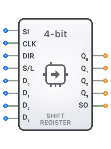
- Symbol: The Shift Register is represented by a rectangular block with inputs for data (serial and sometimes parallel), clock, reset, and mode control, with outputs for the stored/shifted data.
- DigiSim.io Role: Serves as an essential component for data conversion between serial and parallel formats, data storage, and signal processing applications in digital circuit designs.
Functional Description
Logic Behavior
The Shift Register stores and manipulates binary data by shifting the stored bits in a specified direction with each clock pulse. Depending on the type, it can load data serially (one bit at a time) or in parallel (all bits simultaneously), and can output data in either serial or parallel format.
Typical Operation Modes:
| Mode Control | Function | Description |
|---|---|---|
| 00 | Hold | Maintain current state |
| 01 | Shift Right | Move bits right, new bit enters from left |
| 10 | Shift Left | Move bits left, new bit enters from right |
| 11 | Parallel Load | Load all bits simultaneously |
Example Truth Table (4-bit Universal Shift Register):
| CLK | DIR | S/L | SI | D3 | D2 | D1 | D0 | Q3 (Next) | Q2 (Next) | Q1 (Next) | Q0 (Next) | Notes |
|---|---|---|---|---|---|---|---|---|---|---|---|---|
| ↑ | X | 1 | X | d3 | d2 | d1 | d0 | d3 | d2 | d1 | d0 | Parallel Load |
| ↑ | 0 | 0 | si | X | X | X | X | si | Q3 | Q2 | Q1 | Shift Right |
| ↑ | 1 | 0 | si | X | X | X | X | Q2 | Q1 | Q0 | si | Shift Left |
| ↓ | X | X | X | X | X | X | X | Q3 | Q2 | Q1 | Q0 | No Change |
Note: ↑ represents a rising clock edge, ↓ falling edge, X don't care, si serial input, dn parallel data input. Qn is current state.
Inputs and Outputs
Inputs (8 total):
- SI (Serial Input): 1-bit input for serial data entry.
- CLK (Clock): 1-bit input; operations occur on the rising edge.
- DIR (Direction): 1-bit input; controls shift direction (0 = Right, 1 = Left) when S/L is 0.
- S/L (Shift/Load): 1-bit input; mode control (0 = Shift, 1 = Parallel Load).
- D0, D1, D2, D3: Four 1-bit parallel data inputs for loading data simultaneously when S/L is 1.
Outputs (5 total):
- Q0, Q1, Q2, Q3: Four 1-bit parallel outputs representing the current stored bits of the register.
- SO (Serial Output): 1-bit output. Behavior depends on shift direction:
- During Right Shift (DIR=0): SO typically reflects Q0.
- During Left Shift (DIR=1): SO typically reflects Q3.
Configurable Parameters
- Bit Width: The number of bits the shift register can store (typically 4, 8, 16, etc.).
- Shift Direction: Whether the register shifts left, right, or is bidirectional.
- Type: The configuration of the register (SISO, SIPO, PISO, PIPO, or Universal).
- Clock Edge Sensitivity: Whether the register responds to rising or falling clock edges.
- Propagation Delay: The time it takes for outputs to change after a triggering event.
Visual Representation in DigiSim.io
The Shift Register is displayed as a rectangular block with labeled inputs on the left side (SI, D0-D3, CLK, DIR, S/L) and outputs (Q0-Q3, SO) on the right side. The clock input is typically marked with a triangle symbol indicating edge sensitivity. When connected in a circuit, the component visually indicates its current state through the values shown on its outputs and color changes on connecting wires.
Educational Value
Key Concepts
- Sequential Data Processing: Demonstrates how data can be processed one bit at a time in sequence.
- Serial-Parallel Conversion: Illustrates the transformation between sequential and simultaneous data formats.
- Temporal Storage: Shows how digital systems can store and delay data over time.
- Clocked Operation: Reinforces understanding of synchronous digital systems.
- Digital Communication: Introduces fundamental concepts in digital data transmission.
Learning Objectives
- Understand the principles of sequential data storage and manipulation.
- Learn how digital systems convert between serial and parallel data formats.
- Recognize different types of shift registers and their applications.
- Apply shift register concepts to solve data handling problems in digital circuits.
- Comprehend the role of shift registers in digital communication protocols.
Usage Examples/Scenarios
- Serial Communication: Converting between parallel data in a microprocessor and serial data for transmission.
- Delay Lines: Creating precise digital delays for signal processing applications.
- Data Buffering: Temporarily storing data bits before they are processed.
- Pattern Generation: Creating repeating bit patterns for testing or display purposes.
- Digital Filters: Implementing Finite Impulse Response (FIR) filters for signal processing.
- Display Drivers: Controlling LED/LCD matrix displays with limited control lines.
Technical Notes
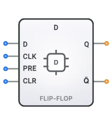
- Shift registers are typically implemented using D flip-flops, with one flip-flop per bit of storage.
- The maximum operating frequency is limited by the propagation delay through the flip-flop chain.
- Universal shift registers offer the most flexibility but require more control inputs and internal logic.
- Linear Feedback Shift Registers (LFSRs) are special configurations used for pseudorandom number generation and CRC calculations.
- In DigiSim.io, shift registers model typical edge-triggered behavior with clear visual feedback of shifting operations.
- Multiple shift registers can be cascaded to handle larger data widths than a single component provides.
Types of Shift Registers
Serial-In, Serial-Out (SISO)
- Data enters one bit at a time and exits one bit at a time
- Acts as a delay line or digital memory element
Serial-In, Parallel-Out (SIPO)
- Data enters serially but can be accessed in parallel
- Used for serial-to-parallel conversion
- Common in communication interfaces (UART, SPI)
Parallel-In, Serial-Out (PISO)
- Data loads in parallel but shifts out serially
- Used for parallel-to-serial conversion
- Essential in data transmission systems
Parallel-In, Parallel-Out (PIPO)
- Data enters and exits in parallel
- Provides temporary storage and can shift data
- Used for data buffering between systems
Bidirectional Shift Registers
- Can shift data left or right
- Allows flexible data manipulation
Universal Shift Registers
- Supports multiple operating modes (all the above)
- Configurable through control inputs
- Provides maximum flexibility
Operation Modes
| Mode Control (S/L, DIR) | Function | Description |
|---|---|---|
| 1, X | Parallel Load | Q[3:0] = D[3:0] |
| 0, 0 | Shift Right | SI → Q3, Q3 → Q2, Q2 → Q1, Q1 → Q0 |
| 0, 1 | Shift Left | Q2 → Q3, Q1 → Q2, Q0 → Q1, SI → Q0 |
Truth Table (4-bit Universal Shift Register)
| CLK | DIR | S/L | SI | D3 | D2 | D1 | D0 | Q3 (Next) | Q2 (Next) | Q1 (Next) | Q0 (Next) | Notes |
|---|---|---|---|---|---|---|---|---|---|---|---|---|
| ↑ | X | 1 | X | d3 | d2 | d1 | d0 | d3 | d2 | d1 | d0 | Parallel Load |
| ↑ | 0 | 0 | si | X | X | X | X | si | Q3 | Q2 | Q1 | Shift Right |
| ↑ | 1 | 0 | si | X | X | X | X | Q2 | Q1 | Q0 | si | Shift Left |
| ↓ | X | X | X | X | X | X | X | Q3 | Q2 | Q1 | Q0 | No Change |
Note: ↑ represents a rising clock edge, ↓ falling edge, X don't care, si serial input, dn parallel data input. Qn is current state.
Characteristics
- Bit Capacity: Typically 4, 8, or 16 bits (can be any length)
- Shift Direction: Left/right/bidirectional depending on configuration
- Clock Requirements: Synchronous operation on clock edges
- Timing: Propagation delay limits maximum shift frequency
- Sampling: Input data sampled at active clock edge
- Reset Behavior: Typically clears all bits to zero
- Preset Options: Some registers allow setting to initial values
- Data Flow Control: May include enable/disable functions
- Power Requirements: Proportional to number of flip-flops and clock frequency
Applications
Data Conversion
- Serial-to-parallel and parallel-to-serial conversion
- Interface between serial buses and parallel processors
Digital Communication
- UART, SPI, I2C interfaces
- Encoding/decoding operations
- Bit framing and data formatting
Signal Processing
- Digital filters (FIR filters)
- Delay lines for digital signal processing
- Correlation and convolution operations
Data Storage
- Temporary buffer storage
- Bit pattern generation and recognition
Computing Systems
- CPU shift/rotate operations
- CRC generation and checking
- Pseudorandom sequence generation
Display Systems
- LED/LCD display multiplexing
- Scrolling displays
- Display panel data distribution
Timing and Control
- Sequence generation
- Event timing and control
Implementation
Shift registers can be implemented using:
Flip-Flop Chains:
- D flip-flops (most common)
- JK flip-flops
- Master-slave configurations
Integrated Circuits:
- 74xx series:
- 7491: 8-bit SISO
- 74164: 8-bit SIPO
- 74165: 8-bit PISO
- 74194/74195: 4-bit universal/4-bit parallel-access
- 74299: 8-bit universal
- 74xx series:
Memory-Based:
- FIFO memory configurations
- Ring buffer implementations
- Shift register LUTs in FPGAs
Circuit Implementation
A basic 4-bit serial-in, serial-out shift register:
### Serial-In Serial-Out (SISO) Shift Register

```mermaid
graph LR
    SIN[Serial In] --> FF0[D FF0]
    CLK[Clock CLK] --> FF0
    FF0 -->|Q0| FF1[D FF1]
    CLK --> FF1
    FF1 -->|Q1| FF2[D FF2]
    CLK --> FF2
    FF2 -->|Q2| FF3[D FF3]
    CLK --> FF3
    FF3 -->|Q3| SOUT[Serial Out]
Related Components
- Registers: General-purpose data storage
- Counters: Sequential circuits that count pulses
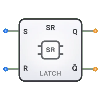
- Flip-Flops: Basic building blocks for shift registers (D, JK)
- Multiplexers: Often used in universal shift register designs
- Serial Communication Interfaces: UART, SPI, I2C
- Linear Feedback Shift Registers: For pseudorandom sequence generation
- Barrel Shifters: For multi-bit shifts in a single cycle
- FIFO/LIFO Buffers: Advanced data storage structures
- Digital Filters: Use shift registers for implementing delay lines
- Sequence Detectors: Pattern recognition circuits