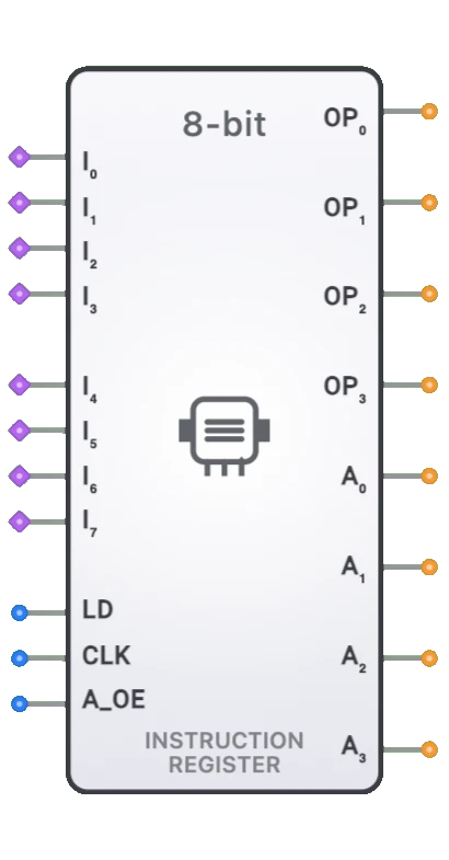
8-Bit Data Bus
Overview
- Purpose: The 8-Bit Data Bus is a visual and functional component that represents a shared data pathway in CPU architectures. It accepts multiple tri-state inputs (bus inputs) and outputs the resolved bus value. The component helps users understand bus architecture and debug bus contention issues.
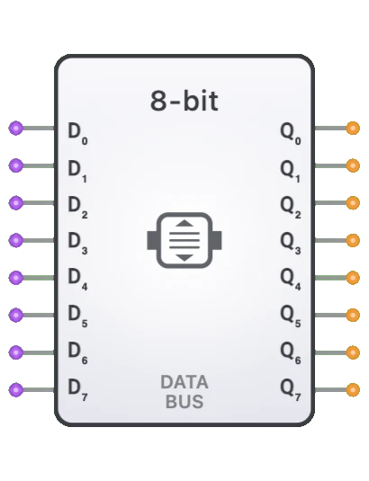
- Symbol: The Data Bus is represented by an elongated rectangular block with 8-bit input and output buses, with internal lines showing the data flow path.
- DigiSim.io Role: Provides a visual representation of bus connections in CPU designs, making it easier to understand data flow and debug issues like bus contention or floating inputs.
Functional Description
Logic Behavior
The 8-Bit Data Bus is primarily a pass-through component that accepts multiple inputs (configured as bus inputs) and outputs the resolved value. The actual tri-state arbitration is handled by DigiSim's event-driven simulator:
- When exactly one driver is active, the output reflects that driver's value.
- When no drivers are active (all high-Z), the outputs are high-Z.
- When multiple drivers are active with conflicting values, bus contention is detected and logged.
Function Table:
| Active Drivers | Driver Values | Q0-Q7 Output | Status |
|---|---|---|---|
| 0 | All High-Z | High-Z | No driver |
| 1 | Value V | V | Normal |
| 2+ (same) | All same | V | Warning |
| 2+ (conflict) | Different | Undefined | Contention! |
Note: Bus contention is logged by the simulator and may indicate a design error
Inputs and Outputs
Inputs:
- D0-D7[7:0]: 8-bit data inputs configured as bus inputs. Multiple tri-state sources can connect to each pin, with the simulator resolving the actual value.
Outputs:
- Q0-Q7[7:0]: 8-bit data outputs that reflect the resolved bus value. Outputs go high-Z when all corresponding inputs are high-Z.
Pin Layout
Input Pins (Left Side):
- Pins 0-7: D0-D7 (Bus inputs - accept multiple tri-state connections)
Output Pins (Right Side):
- Pins 0-7: Q0-Q7 (Resolved bus value outputs)
Configurable Parameters
- Contention Detection: Automatic detection and logging of bus conflicts.
- Propagation Delay: Minimal delay for signal pass-through.
Visual Representation in DigiSim.io
The 8-Bit Data Bus is displayed as a rectangular block (112x160 pixels) with:
- 8 input pins on the left side (D0-D7), marked as bus inputs
- 8 output pins on the right side (Q0-Q7)
- Internal horizontal lines showing data flow
- Labels "DATA BUS" and "8-BIT" in the center
The thicker bus input pins indicate that multiple tri-state sources can connect, distinguishing them from regular single-source inputs.
Educational Value
Key Concepts
- Bus Architecture: Demonstrates how multiple components share a common data pathway.
- Tri-State Logic: Shows how tri-state outputs enable bus sharing without multiplexers.
- Bus Contention: Illustrates potential conflicts when multiple drivers are active.
- Data Flow Visualization: Makes abstract bus concepts tangible and visible.
- Modular Design: Encourages thinking about CPU components as separate modules communicating via buses.
Learning Objectives
- Understand how data buses enable component communication in CPUs.
- Learn the importance of bus arbitration and control signals.
- Recognize bus contention as a common design error and how to avoid it.
- Apply bus architecture concepts in designing modular digital systems.
- Comprehend the role of tri-state buffers in bus-based designs.
Usage Examples/Scenarios
- CPU Data Path: Central data bus connecting ALU, registers, and memory.
- Memory Data Interface: Bidirectional data flow between CPU and RAM/ROM.
- Register File: Common bus for reading/writing multiple registers.
- I/O Interface: Data exchange between CPU and peripheral devices.
- Debug and Visualization: Making bus signals visible for troubleshooting.
Integration in 8-Bit Computer
In the DigiSim 8-bit computer architecture, the Data Bus connects all major components:
┌──────────────────────────────────────────────────────────────────┐
│                     8-BIT DATA BUS                                │
│                                                                   │
│  ┌─────────┐  ┌─────────┐  ┌─────────┐  ┌─────────┐  ┌────────┐ │
│  │   ACC   │  │   ALU   │  │   RAM   │  │   ROM   │  │   IR   │ │
│  │         │  │         │  │         │  │         │  │        │ │
│  └────┬────┘  └────┬────┘  └────┬────┘  └────┬────┘  └───┬────┘ │
│       │            │            │            │           │       │
│       ▼            ▼            ▼            ▼           ▼       │
│  ┌────────┐  ┌────────┐  ┌────────┐  ┌────────┐  ┌────────┐    │
│  │TRI-BUF │  │TRI-BUF │  │TRI-BUF │  │TRI-BUF │  │TRI-BUF │    │
│  │(ACC_OE)│  │(ALU_OE)│  │(RAM_OE)│  │(ROM_OE)│  │(IR_OE) │    │
│  └────┬────┘  └────┬────┘  └────┬────┘  └────┬────┘  └───┬────┘ │
│       │            │            │            │           │       │
│       └────────────┴────────────┴─────┬──────┴───────────┘       │
│                                       │                          │
│                              ┌────────▼────────┐                 │
│                              │    DATA BUS     │                 │
│                              │     8-BIT       │                 │
│                              └────────┬────────┘                 │
│                                       │                          │
│       ┌───────────────────────────────┼───────────────────┐      │
│       ▼                               ▼                   ▼      │
│  ┌─────────┐                    ┌─────────┐         ┌─────────┐ │
│  │   ACC   │                    │   RAM   │         │   MAR   │ │
│  │  (IN)   │                    │  (DIN)  │         │  (DIN)  │ │
│  └─────────┘                    └─────────┘         └─────────┘ │
│                                                                   │
└──────────────────────────────────────────────────────────────────┘
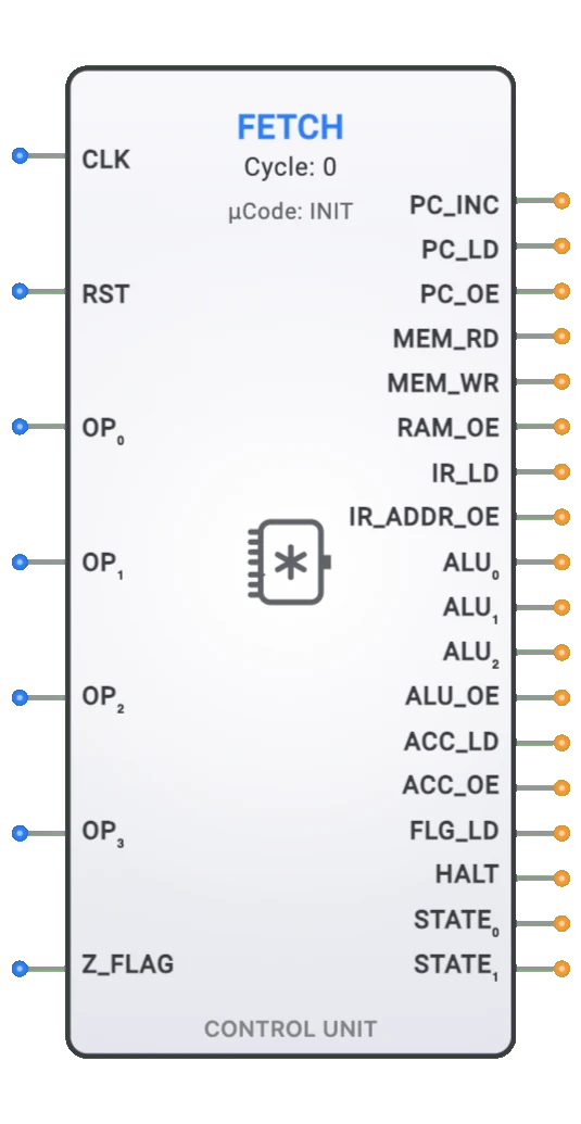
Control Signal Coordination
The Control Unit ensures only one driver is active at any time:
| Microcode Step | Active Driver | Control Signal |
|---|---|---|
| Fetch Instruction | ROM | ROM_OE = 1 |
| Load from RAM | RAM | RAM_OE = 1 |
| ALU Result | ALU | ALU_OE = 1 |
| ACC Output | Accumulator | ACC_OE = 1 |
| Immediate Load | IR (operand) | IR_OE = 1 |
Technical Notes
- The Data Bus component is primarily visual - the simulator handles actual bus arbitration.
- Bus inputs are marked with
isBusInput: truein the component configuration. - The
resolveBusContentionfunction in the simulator handles multiple driver scenarios. - Each bit of the bus is resolved independently.
- High-Z (floating) inputs propagate as high-Z outputs.
- Contention detection helps identify timing issues where multiple drivers overlap.
- In physical circuits, bus contention can cause excessive current and potential damage.
Debugging Bus Issues
Common Problems
- All Outputs High-Z: No driver is enabled. Check output enable signals.
- Unexpected Values: Wrong driver enabled. Verify control signal timing.
- Contention Warnings: Multiple drivers active. Check mutual exclusion in control logic.
- Intermittent Errors: Timing issues. Ensure proper sequencing of enable signals.
Debugging Tips
- Use the oscilloscope to observe output enable signals.
- Verify only one OE signal is active during each clock phase.
- Check that OE signals are properly synchronized with clock.
- Use the Data Bus component's visual state to see active/inactive status.
Related Components
- Accumulator: Connects to data bus for arithmetic operations.
- ALU (8-bit): Provides computation results to data bus.
- RAM: Reads/writes data via the bus.
- ROM: Provides instruction data to the bus.
- Instruction Register (IR): Receives instructions from bus, outputs operands.
- Memory Address Register (MAR): May receive addresses from data bus.
- Tri-State Buffer (8-bit): Gates component outputs onto the bus.
- Control Unit: Coordinates which component drives the bus.