Half Adder
Overview
- Purpose: The Half Adder is a digital combinational circuit that performs the addition of two binary digits (bits). It produces a sum output and a carry output, representing the result of adding two bits.
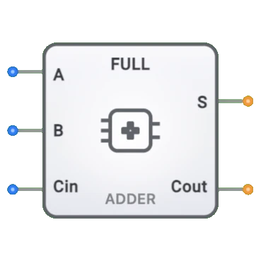
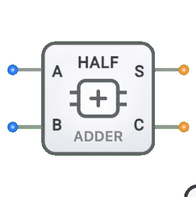
- Symbol: The Half Adder is represented by a rectangular block labeled "HA" with two inputs (A and B) and two outputs (Sum and Carry).
- DigiSim.io Role: Serves as a fundamental building block for arithmetic operations, forming the basis for more complex digital adders and binary calculators.
Functional Description
Logic Behavior
The Half Adder performs binary addition of two single bits, generating two outputs: Sum (the result bit) and Carry (the overflow bit).
Truth Table:
| Input A | Input B | Sum (S) | Carry (C) |
|---|---|---|---|
| 0 | 0 | 0 | 0 |
| 0 | 1 | 1 | 0 |
| 1 | 0 | 1 | 0 |
| 1 | 1 | 0 | 1 |
Boolean Expressions:
- Sum (S) = A ⊕ B (XOR operation)
- Carry (C) = A · B (AND operation)
Inputs and Outputs
- Inputs:
- Input A: 1-bit first binary input.
- Input B: 1-bit second binary input.
- Outputs:
- Sum (S): 1-bit sum output representing the modulo-2 sum of inputs.
- Carry (C): 1-bit carry output representing the overflow when both inputs are 1.
Configurable Parameters
- Propagation Delay: The time it takes for the outputs to change after input changes. DigiSim.io simulates this delay in the event-driven simulator.
Visual Representation in DigiSim.io
The Half Adder is displayed as a rectangular block with inputs on the left side and outputs on the right side. It is labeled to identify it as a Half Adder. When connected in a circuit, the component visually indicates the logic state of its pins through color changes on connecting wires.
Educational Value
Key Concepts
- Binary Arithmetic: Demonstrates the fundamental process of binary addition.
- Combinational Logic: Shows how complex operations can be built from basic logic gates.
- Multi-Output Circuits: Illustrates how a circuit can produce multiple outputs from the same inputs.
- Building Block Design: Introduces the concept of using simple components to create more complex systems.
Learning Objectives
- Understand the basic principles of binary addition.
- Learn how XOR and AND gates combine to form a Half Adder.
- Recognize the Half Adder's role in building more complex arithmetic circuits.
- Apply Half Adders to design simple binary calculators and counters.
Usage Examples/Scenarios
- Binary Addition: Performing the most basic single-bit addition operation.
- Counter Circuits: Used as a component in binary counter designs.
- Full Adder Construction: Two Half Adders combined with an OR gate form a Full Adder.
- ALU Components: Serving as a building block in Arithmetic Logic Units.
- Binary Calculators: Creating simple binary calculator circuits.
Technical Notes
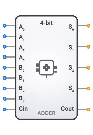
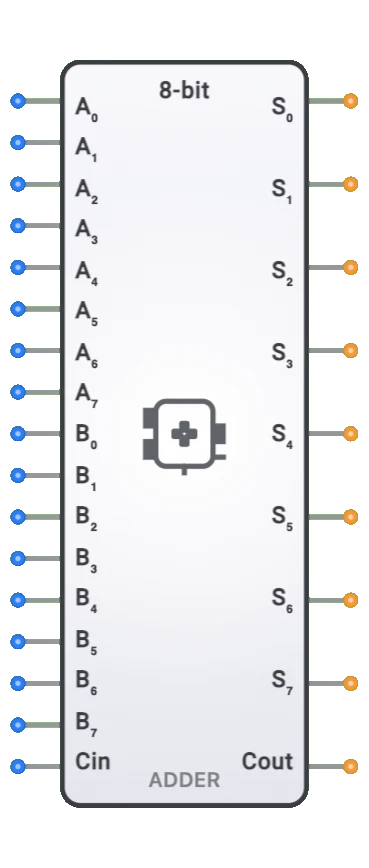
- The Half Adder cannot process a carry input from a previous addition operation, limiting its use in multi-bit addition without modification.
- For multi-bit binary addition, multiple Half Adders or Full Adders must be cascaded.
- The Sum output is effectively an XOR operation, while the Carry output is an AND operation.
- In physical implementations, the Carry output typically has a slightly shorter propagation delay than the Sum output.
Characteristics
- Propagation Delay:
- Sum: Typically 10-20ns (technology dependent)
- Carry: Typically 5-15ns (usually faster than the sum)
- Power Consumption: Low
- Fan-Out: Typically 10-50 gates (technology dependent)
- Number of Gates: Requires 2 basic gates (1 XOR and 1 AND)
- Circuit Complexity: Low
- Noise Margin: Moderate to high (depends on implementation technology)
Implementation Methods
Using Basic Logic Gates
- XOR gate for the Sum output
- AND gate for the Carry output
Transistor-Level Implementation
- CMOS: Using complementary MOSFETs
- TTL: Using bipolar junction transistors
- Can be optimized for speed or power
Integrated Circuits
- Available in 74xx series logic families
- Often incorporated into larger adder chips
- Also available as part of ALU (Arithmetic Logic Unit) circuits
FPGA/CPLD Implementation
- Uses lookup tables (LUTs) or dedicated adder logic
- Can be optimized for performance or resource utilization
Circuit Implementation
Basic gate-level implementation of a half adder:
graph LR
    InputA[Input A] --> XorGate[XOR Gate]
    InputB[Input B] --> XorGate
    XorGate --> SumOut[Sum S]

    InputA --> AndGate[AND Gate]
    InputB --> AndGate
    AndGate --> CarryOut[Carry C]
Logic:
- Sum (S) = A ⊕ B: XOR produces 1 when inputs differ
- Carry (C) = A · B: AND produces 1 only when both inputs are 1
Applications
Building Block for Full Adders
- Two half adders and an OR gate can be used to construct a full adder
- Forms the basis for multi-bit adders
Binary Counters
- Used in sequential counter circuits
- Used for address generation in digital systems
Arithmetic Logic Units (ALUs)
- Fundamental component in CPU arithmetic operations
- Used for addition operations in processors
Digital Signal Processing
- Used in digital filters and signal processors
- Component in multiply-accumulate operations
Error Detection/Correction Circuits
- Used in parity generators and checkers
- Component in checksums and CRC calculations
Limitations
No Carry Input
- Cannot handle a carry from a previous addition
- Requires a full adder for multi-bit addition
Two-Input Restriction
- Limited to adding only two binary digits
- Multiple half adders needed for multi-bit numbers
Related Components
- Full Adder: Extends the half adder with a carry input
- Ripple Carry Adder: Multiple full adders connected in series
- Look-ahead Carry Adder: Advanced adder with faster carry propagation
- Binary Counter: Sequential circuit using adders for counting
- Arithmetic Logic Unit (ALU): Incorporates adders for mathematical operations