D Latch
Overview
- Purpose: The D Latch (Data Latch) is a level-sensitive memory circuit that stores a single bit of information. It improves upon the SR latch by using a single data input (D) to eliminate invalid states, while an enable input controls when the latch accepts new data.
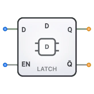
- Symbol: The D Latch is represented by a rectangular block with inputs for D (data) and EN (enable), and complementary outputs Q and Q̅.
- DigiSim.io Role: Serves as a fundamental building block for memory storage in digital circuits, providing temporary data holding and demonstrating level-sensitive behavior as opposed to edge-triggered operation.
Functional Description
Logic Behavior
The D Latch is transparent when enabled, passing the D input value to the Q output. When disabled, it maintains (latches) its last state regardless of changes to the D input.
Truth Table:
| Enable (EN) | Data (D) | Q (next) | Operation |
|---|---|---|---|
| 0 | X | Q (prev) | Hold state |
| 1 | 0 | 0 | Reset (Load 0) |
| 1 | 1 | 1 | Set (Load 1) |
Note: X represents "don't care" condition, "prev" means previous state
Inputs and Outputs
Inputs:
- D (Data): 1-bit input that provides the value to be stored when the latch is enabled.
- EN (Enable): 1-bit control input that determines when the latch is transparent (EN=1) or holding (EN=0).
Outputs:
- Q: 1-bit output representing the stored value.
- Q̅: 1-bit complementary output representing the inverse of the stored value.
Configurable Parameters
- Active Level: Whether the enable input is active-high or active-low.
- Propagation Delay: The time it takes for outputs to change after input or enable changes.
Visual Representation in DigiSim.io
The D Latch is displayed as a rectangular block with labeled inputs on the left side (D and EN) and outputs (Q and Q̅) on the right side. When connected in a circuit, the component visually indicates its current state through the values shown on its outputs and color changes on connecting wires. The transparency or holding behavior is also visually indicated when the enable input changes state.
Educational Value
Key Concepts
- Level Sensitivity: Demonstrates how circuits respond to signal levels rather than edges.
- Transparency and Latching: Illustrates the concepts of transparent (pass-through) and memory (holding) modes.
- Memory Storage: Shows how digital circuits can store information temporarily.
- Signal Timing: Introduces the importance of setup and hold times in digital memory elements.
- Data Synchronization: Demonstrates how data can be captured at specific times for synchronization purposes.
Learning Objectives
- Understand the difference between level-sensitive latches and edge-triggered flip-flops.
- Learn how the enable input controls when data is captured versus maintained.
- Recognize the timing considerations for reliable data capture in latches.
- Apply D latches in designing simple memory circuits and data holding registers.
- Comprehend how latches can be used in two-phase clocking schemes and transparent registers.
Usage Examples/Scenarios
- Data Registers: Temporarily storing multi-bit data values when enable is activated.
- Input Capture: Sampling input data at specific times by controlling the enable signal.
- Bus Interfaces: Holding address or data values steady during bus transfers.
- Two-Phase Clocking: Creating pipeline stages in alternating latch systems.
- Time Borrowing: Allowing operations to extend across clock boundaries in pipelined systems.
- Level-Sensitive Scan Design: Supporting circuit testing by creating controllable scan chains.
Technical Notes
- Unlike edge-triggered flip-flops, D latches are transparent whenever the enable input is active, making timing control more critical.
- Multiple transitions on the D input while enable is active will cause multiple transitions on the output, which can lead to race conditions in certain designs.
- The "transparency window" of a latch can be advantageous for time borrowing in pipeline designs but requires careful timing analysis.
- D latches typically require less logic than edge-triggered flip-flops, potentially offering faster operation but with more timing constraints.
- In DigiSim.io, the D Latch clearly demonstrates the difference between level-sensitive and edge-triggered behavior, an important concept in digital design.
Characteristics
- Memory Property:
- Stores the value present at D input when Enable transitions from high to low
- Transparent when Enable is high (level-sensitive)
- Propagation Delay:
- Data-to-Q delay (when enabled): Typically 5-15ns (technology dependent)
- Enable-to-output delay: Typically 5-15ns (technology dependent)
- Setup and Hold Times:
- Setup time: Time D must be stable before Enable goes low
- Hold time: Time D must be stable after Enable goes low
- Power Consumption:
- Static: Low (mainly leakage current)
- Dynamic: Moderate during state changes
- Fan-Out:
- Typically 10-50 gates (technology dependent)
- Circuit Complexity:
- Medium (requires an SR latch plus input gating logic)
- Speed:
- Faster than edge-triggered flip-flops but requires longer setup and hold times
- Noise Margin:
- Moderate (depends on gate technology)
- Operational Modes:
- Transparent mode (when Enable is high)
- Memory mode (when Enable is low)
Implementation Methods
- Using an SR Latch with Input Gating
graph TB
    D[D Input] --> AND1[AND Gate]
    EN[Enable] --> AND1
    EN --> AND2[AND Gate]

    D --> NOT[NOT Gate]
    NOT --> AND2

    AND1 -->|S| SR[SR Latch]
    AND2 -->|R| SR

    SR --> Q[Q Output]
    SR --> QB[Q̅ Output]
Operation: When Enable=1, D passes through to Set (if D=1) or Reset (if D=0). When Enable=0, latch holds state.
- Using NAND Gates
graph TB
    D[D Input] --> NAND1[NAND Gate]
    EN[Enable] --> NAND1
    EN --> NAND2[NAND Gate]

    D --> NOT[NOT Gate]
    NOT --> NAND2

    NAND1 --> NAND3[NAND Latch]
    NAND2 --> NAND4[NAND Latch]

    NAND3 --> Q[Q Output]
    NAND3 --> NAND4
    NAND4 --> QB[Q̅ Output]
    NAND4 --> NAND3
Operation: NAND-based implementation with cross-coupled feedback for memory.
Transistor-Level Implementation
- CMOS: Using transmission gates and inverters
- TTL: Using bipolar junction transistors
- Can be optimized for power, speed, or area
Integrated Circuits
- Available in 74xx series logic families (e.g., 74HC75, 74LS373)
- Often organized as quad or octal latches in a single package
Applications
Data Storage
- Temporary storage registers in data paths
- I/O port latches in microprocessors
- Address latches in memory systems
Data Synchronization
- Holding data stable between asynchronous domains
- Input capture in data acquisition systems
Level-Sensitive Scan Design (LSSD)
- Design for testability in digital systems
- Scan chains for fault detection
Pipeline Registers
- Transparent latches in two-phase clocking systems
- Time-borrowing across pipeline stages
Data Demultiplexing
- Holding demultiplexed data in time-division systems
- Sample-and-hold circuits in digital systems
Bus Interface Circuits
- Data bus latches
- Address latches in memory interfaces
Limitations
Transparency Window
- Susceptible to multiple transitions during enable high period
- Cannot reliably capture short pulses
Level Sensitivity
- Changes to input during enable high period pass to output
- Potential for unwanted feedback and oscillation
Timing Constraints
- Setup and hold time requirements can be challenging
- Risk of metastability if data changes near enable transition
Clock Skew Sensitivity
- In multi-latch systems, enable skew can cause race conditions
- More difficult to manage in complex systems than edge-triggered circuits
Limited Protection Against Noise
- Data glitches during enable high period propagate to output
- More susceptible to noise than edge-triggered flip-flops
Circuit Implementation Detail
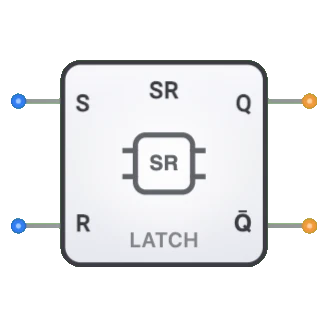
D Latch from SR Latch
The D Latch can be constructed from an SR Latch by ensuring that the S and R inputs are never both high at the same time:
S = D · EN
R = (¬D) · EN
When EN is high, either S or R will be high (but never both) depending on D. When EN is low, both S and R are low, placing the SR latch in its hold state.
Gated D Latch Behavior
When EN = 0:
- Both S and R inputs to the internal SR latch are 0
- The latch maintains its previous state
When EN = 1:
- If D = 1: S = 1, R = 0, and the latch sets Q to 1
- If D = 0: S = 0, R = 1, and the latch resets Q to 0
- The output follows the D input (transparent mode)
Related Components
- SR Latch: The foundational latch that D Latch is built upon
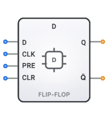
- D Flip-Flop: Edge-triggered version of the D latch for synchronous systems
- JK Flip-Flop: More versatile flip-flop with set, reset, and toggle capabilities
- T Flip-Flop: Toggle flip-flop that changes state on clock edges
- Transparent Latch: Another name for the D latch emphasizing its behavior
- Register: Multiple latches organized to store multi-bit values
- Master-Slave Flip-Flop: Two latches in series creating edge-triggered behavior