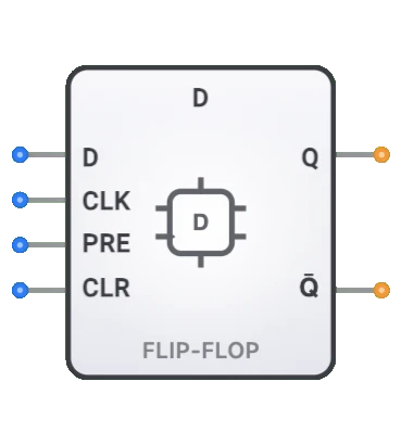
JK Flip-Flop
Overview
- Purpose: The JK Flip-Flop is a sequential digital circuit that stores one bit of data and offers versatile state control. It improves upon the SR Flip-Flop by eliminating invalid states and adding a toggle functionality when both inputs are HIGH.
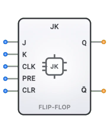
- Symbol: The JK Flip-Flop is represented by a rectangular block with inputs for J (set), K (reset), Clock (CLK), and sometimes asynchronous SET and RESET, with outputs Q and Q̅.
- DigiSim.io Role: Serves as a fundamental memory element in sequential digital circuits, providing a versatile building block for counters, registers, state machines, and control applications.
Functional Description
Logic Behavior
The JK Flip-Flop changes state based on the J and K inputs when triggered by a positive clock edge (rising edge). It features asynchronous preset and clear inputs that can override the normal operation.
Pin Layout:
- Pin 0: J (Set control input)
- Pin 1: K (Reset control input)
- Pin 2: CLK (Clock input)
- Pin 3: PRE (Preset - asynchronous set)
- Pin 4: CLR (Clear - asynchronous reset)
- Output 0: Q (stored value)
- Output 1: Q̅ (complementary output)
Truth Table (Positive Edge-Triggered JK Flip-Flop):
| PRE | CLR | J | K | CLK | Q (next) | Q̅ (next) | Operation |
|---|---|---|---|---|---|---|---|
| 0 | 1 | X | X | X | 0 | 1 | Asynchronous Clear |
| 1 | 0 | X | X | X | 1 | 0 | Asynchronous Preset |
| 0 | 0 | 0 | 0 | ↑ | Q (prev) | Q̅ (prev) | No change (hold) |
| 0 | 0 | 0 | 1 | ↑ | 0 | 1 | Reset |
| 0 | 0 | 1 | 0 | ↑ | 1 | 0 | Set |
| 0 | 0 | 1 | 1 | ↑ | Q̅ (prev) | Q (prev) | Toggle |
| 0 | 0 | X | X | 0 | Q (prev) | Q̅ (prev) | Hold previous state |
| 0 | 0 | X | X | ↓ | Q (prev) | Q̅ (prev) | Hold previous state |
Note: ↑ indicates rising edge of clock, ↓ indicates falling edge, X means "don't care", 0 = inactive (LOW), 1 = active (HIGH)
Operation Priority (highest to lowest):
- CLR (Clear): When CLR=1, Q is forced to 0 regardless of other inputs
- PRE (Preset): When PRE=1 and CLR=0, Q is forced to 1 regardless of other inputs
- Clock Edge: When PRE=0 and CLR=0, J and K inputs control state on rising clock edge
Inputs and Outputs
Inputs:
- J [Pin 0]: 1-bit "Set control" input that works with K to determine the flip-flop's next state.
- K [Pin 1]: 1-bit "Reset control" input that works with J to determine the flip-flop's next state.
- CLK (Clock) [Pin 2]: 1-bit positive-edge timing signal that triggers state changes.
- PRE (Preset) [Pin 3]: 1-bit asynchronous input that forces Q to 1 when active HIGH.
- CLR (Clear) [Pin 4]: 1-bit asynchronous input that forces Q to 0 when active HIGH (highest priority).
Outputs:
- Q: 1-bit output representing the stored bit (current state).
- Q̅: 1-bit output representing the complement of the stored bit.
Configurable Parameters
- Clock Edge Sensitivity: Whether the flip-flop responds to rising or falling clock edges.
- Asynchronous Inputs: Whether SET and RESET inputs are present.
- Propagation Delay: The time it takes for outputs to change after a triggering event.
Visual Representation in DigiSim.io
The JK Flip-Flop is displayed as a rectangular block with labeled inputs on the left side (J, K, CLK, PRE, CLR from top to bottom) and outputs (Q and Q̅) on the right side. The component is clearly labeled with "JK FF" to identify it as a JK Flip-Flop. The clock input is typically marked with a triangle symbol indicating positive-edge sensitivity. When connected in a circuit, the component visually indicates its current state through the values shown on its outputs and color changes on connecting wires.
Educational Value
Key Concepts
- Sequential Logic: Demonstrates how circuits can store and change state based on timing signals.
- Edge-Triggered Behavior: Illustrates how digital circuits can respond to signal transitions rather than levels.
- Feedback Systems: Shows how the current state affects the next state calculation.
- State Memory: Introduces how digital circuits maintain state between clock cycles.
- Toggle Functionality: Demonstrates binary state switching, a fundamental concept in digital counters.
Learning Objectives
- Understand how JK Flip-Flops store binary information and change states.
- Learn the relationship between input combinations and resulting state changes.
- Recognize how the toggle mode enables efficient counter design.
- Apply JK Flip-Flops in designing sequential circuits like counters and state machines.
- Comprehend how JK Flip-Flops can emulate other flip-flop types through appropriate connections.
Usage Examples/Scenarios
- Binary Counters: Utilizing the toggle functionality for counting sequential states.
- Frequency Division: Creating clock dividers by toggling on each input clock pulse.
- Shift Registers: Storing and shifting data bits through a series of flip-flops.
- State Machines: Creating circuits that progress through defined sequences of states.
- Debounce Circuits: Removing noise from mechanical switch inputs.
- Memory Elements: Storing individual bits in memory systems.
Technical Notes
- The JK Flip-Flop's toggle feature (when J=K=1) makes it particularly useful for counter designs.
- JK Flip-Flops can be configured to operate as other flip-flop types:
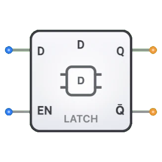
- As a D Flip-Flop: Connect J to D and K to NOT D
- As a T Flip-Flop: Connect J and K together (J=K=T)
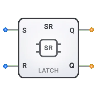
- As an SR Flip-Flop: Use directly, but avoid J=K=1 for pure SR behavior
- Positive edge-triggered JK Flip-Flops have specific setup and hold time requirements for reliable operation.
- Asynchronous Control: PRE and CLR inputs are active-HIGH and take precedence over the synchronous clock inputs. CLR has higher priority than PRE.
- Control Signal Priority: The CLR input always overrides PRE and synchronized inputs. When CLR=1, output is forced to 0. When PRE=1 and CLR=0, output is forced to 1.
- In DigiSim.io, the JK Flip-Flop models positive edge-triggered behavior with clear visual feedback of state transitions.
Timing Diagram
Operation Example:
| Clock Edge | J | K | Action | Q (next) |
|---|---|---|---|---|
| Rising 1 | 0 | 1 | Reset | 0 |
| Rising 2 | 1 | 0 | Set | 1 |
| Rising 3 | 1 | 1 | Toggle | 0 |
| Rising 4 | 1 | 1 | Toggle | 1 |
| Rising 5 | 0 | 0 | Hold | 1 |
Key Behavior: Output changes only on clock edges, providing stable synchronous operation.
Characteristics
- More versatile than SR or D flip-flops
- Provides a toggle function when both J and K are HIGH
- No invalid states during normal operation
- Edge-triggered (responds on clock transition)
- Has setup and hold time requirements
- Can be used as a T flip-flop by connecting J and K together
- Can be used as a D flip-flop with simple logic
Applications
- Counters and frequency dividers (using the toggle feature)
- Shift registers
- State machines
- Memory elements in sequential digital circuits
- Pulse detection and generation
- Debouncing physical switches
- Timing and synchronization circuits
- Toggle switches in digital systems
Implementation
JK Flip-Flops can be constructed from:
- NAND or NOR gates
- A modified master-slave arrangement
- Common IC packages:
- 7473: Dual JK flip-flop with clear
- 7476: Dual JK flip-flop with preset and clear
- 74112: Dual JK flip-flop with preset and clear, negative-edge triggered
Functional Relationships
JK Flip-Flops can be configured as other flip-flop types:
- D Flip-Flop: Connect J to D and K to NOT D
- T Flip-Flop: Connect J and K together (J=K=T)
- SR Flip-Flop: Use directly, but avoid J=K=1 for SR behavior
Circuit Diagram
A basic JK flip-flop can be implemented using NAND gates in a master-slave configuration with feedback paths to provide the toggle functionality.
Related Components
- SR Flip-Flop: Simpler design, but has invalid input combination
- D Flip-Flop: Data storage, no toggle capability
- T Flip-Flop: Toggle-only functionality
- Counter: Often built using JK flip-flops for their toggle capability