Instruction Register (IR)
Overview
- Purpose: The Instruction Register (IR) is a specialized register within a CPU that temporarily holds the machine code instruction fetched from memory while it is being decoded and executed by the control unit.
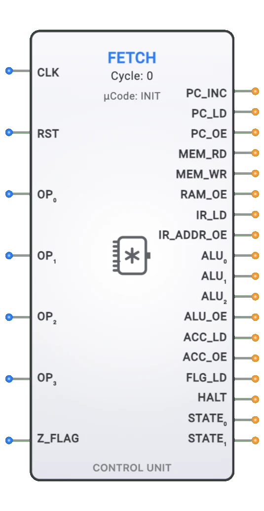
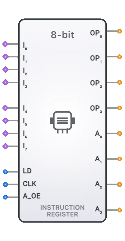
- Symbol: The Instruction Register is represented by a rectangular block with inputs for data from memory, clock, and load enable, with outputs providing the instruction bits to the decoder.
- DigiSim.io Role: Serves as a critical component in CPU designs, linking the fetch and decode stages of the instruction cycle and providing stable access to the instruction's opcode and operands.
Functional Description
Logic Behavior
The Instruction Register captures and holds the instruction data from memory during the fetch cycle, making it available to the instruction decoder throughout the decode and execute cycles. It functions primarily as a storage element with load control.
Function Table:
| LD | CLK | A_OE | Action | Opcode (OP0-OP3) | Address (A0-A3) |
|---|---|---|---|---|---|
| 1 | ↑ | X | Load New Instruction | Loaded Data[3:0] | Loaded Data[7:4] or Hi-Z |
| 0 | ↑ | X | Hold Current Value | Current Value | Current Value or Hi-Z |
| X | 0 | X | No Change | Current Value | Current Value or Hi-Z |
| X | X | 1 | Address Output Enable | Current Value | Current Value |
| X | X | 0 | Address Hi-Z | Current Value | Hi-Z |
Note: ↑ represents a rising clock edge, X represents a "don't care" condition
Inputs and Outputs
Inputs:
- I0-I7: 8-bit data inputs connected to the memory data bus to receive fetched instructions.
- LD: 1-bit load enable input that enables loading of a new instruction when active.
- CLK: 1-bit clock input that synchronizes the loading operation.
- A_OE: 1-bit address output enable that controls whether address bits are driven on outputs.
Outputs:
- OP0-OP3: 4-bit opcode outputs providing the operation code to the control unit (always enabled).
- A0-A3: 4-bit address outputs providing addressing information (controlled by A_OE).
- The opcode outputs are always available once loaded, as the control unit needs immediate access.
- The address outputs can be tri-stated using A_OE for bus sharing during memory operations.
Configurable Parameters
- Register Width: The number of bits the IR can store, matching the CPU's instruction word size.
- Clock Edge Sensitivity: Whether the register responds to rising or falling clock edges.
- Load Behavior: How the load control signal interacts with the clock.
- Propagation Delay: The time it takes for outputs to change after a triggering event.
Visual Representation in DigiSim.io
The Instruction Register is displayed as a rectangular block with labeled inputs on the left side (DATA[n:0], CLK, LOAD) and outputs (IR_OUT[n:0]) on the right side. The clock input is typically marked with a triangle symbol indicating edge sensitivity. When connected in a circuit, the component visually indicates its current state through the instruction value shown on its outputs and color changes on connecting wires.
Educational Value
Key Concepts
- Instruction Cycle: Demonstrates a key stage in the fetch-decode-execute cycle of a CPU.
- Instruction Decoding: Illustrates how machine code instructions are prepared for interpretation.
- CPU Architecture: Introduces a fundamental component in CPU control units.
- Sequential Processing: Shows how data flows through a CPU in discrete stages.
- Instruction Set Architecture: Helps visualize how machine code instructions are handled.
Learning Objectives
- Understand the role of the Instruction Register in the CPU execution cycle.
- Learn how instructions are captured and held stable during CPU operation.
- Recognize how the IR interfaces with memory and the instruction decoder.
- Apply IR concepts in designing simple CPU architectures.
- Comprehend the relationship between instruction formats and CPU organization.
Usage Examples/Scenarios
- Basic CPU Design: Core component in a fetch-decode-execute cycle implementation.
- Instruction Decoding: Providing stable instruction data to the decoder circuitry.
- Pipelined Architecture: Separating the fetch and decode stages in a CPU pipeline.
- Microcode Implementation: Holding instructions while the control unit steps through micro-operations.
- Educational CPU Models: Demonstrating the fundamental principles of CPU operation.
- Hardwired Control Units: Providing instruction bits directly to combinational control logic.
Technical Notes
- The width of the Instruction Register matches the instruction size of the processor architecture.
- The IR is typically loaded during the fetch phase of the instruction cycle.
- In a simple non-pipelined CPU, the IR holds each instruction for its entire execution duration.
- In pipelined architectures, multiple IRs may exist at different pipeline stages.
- The IR's outputs are often split into fields that have specific meanings based on the instruction format.
- Some complex instruction sets require additional logic to handle variable-length instructions.
- The IR isolates the control unit from the data bus, allowing memory to be used for other operations while the current instruction is being executed.
graph LR
    DATA[Data Bus<br/>from Memory] --> IR[Instruction Register]
    CLK[Clock] --> IR
    LOAD[Load Enable] --> IR
    IR --> OUT[Output to Decoder<br/>Opcode & Operands]
Note: The size of the IR matches the instruction size of the architecture. Outputs are routed to the instruction decoder logic.
Truth Table / Function Table
The IR primarily functions as a storage element:
| LOAD | CLK | Action Taken on Clock Edge | IR Output (Next State) |
|---|---|---|---|
| 1 | ↑ | Load Input Data | Input Data |
| 0 | ↑ | Hold Current Value | IR Output (Current) |
| X | 0/↓ | No Change | IR Output (Current) |
The output is typically stable between load operations and continuously available to the instruction decoder.
Characteristics
Input Configuration:
- Data Inputs (I0-I7): 8-bit parallel inputs connected to the memory data bus to receive fetched instructions.
- Load Enable (LD): Control signal asserted during the fetch cycle to latch the instruction.
- Clock Input (CLK): Synchronizes the loading operation on rising edge.
- Address Output Enable (A_OE): Controls tri-state behavior of address outputs for bus sharing.
Output Configuration:
- Opcode Outputs (OP0-OP3): 4-bit outputs providing the operation code, always enabled for immediate access by control unit.
- Address Outputs (A0-A3): 4-bit outputs providing addressing information, can be tri-stated via A_OE.
- Opcode bits are typically routed directly to the control unit for instruction decoding.
- Address bits are used for memory addressing and jump operations when enabled.
Functionality:
- Temporarily stores the currently fetched instruction.
- Holds the instruction stable while it is being decoded and executed.
- Isolates the control unit from changes on the data bus after the fetch cycle.
- Provides the raw instruction bits needed by the instruction decoder.
Propagation Delay:
- Clock-to-output delay: Time for the instruction to be available at the outputs after the clock edge during a load operation.
- Setup/Hold time requirements for the data inputs relative to the clock and load signal.
Circuit Complexity:
- Core: A parallel-in, parallel-out register composed of D flip-flops (one per bit of the instruction width).
- Control logic for the LOAD signal.
Implementation Methods
- Array of D Flip-Flops: The most common method, using one D flip-flop for each bit of the instruction word, clocked simultaneously with a common LOAD signal.
- Standard Register IC: Using off-the-shelf register ICs (e.g., 74HC374, 74HC574 for 8-bit instructions).
- FPGA/ASIC Implementation: Synthesized from HDL code within a larger CPU design.
Applications
- Instruction Decode and Execute Cycle: Central component in the fetch-decode-execute cycle of a CPU.
- CPU Control Unit: Provides the input to the instruction decoder logic, which in turn generates control signals for the rest of the CPU.
- Pipeline Stages: In pipelined processors, the IR often exists within the Instruction Decode (ID) pipeline stage.
Limitations
- Fixed Width: The IR size dictates the maximum instruction size the CPU can handle directly.
- Bottleneck: In some older architectures, fetching into the IR could be a performance bottleneck, addressed by techniques like instruction prefetching and pipelining.
Circuit Implementation Detail
An 8-bit IR implemented with D flip-flops:
graph LR
    D0[Data_In 0] --> FF0[D Flip-Flop 0]
    D1[Data_In 1] --> FF1[D Flip-Flop 1]
    D2[Data_In 2] --> FF2[D Flip-Flop 2]
    D7[Data_In 7] --> FF7[D Flip-Flop 7]

    CLK[Clock] --> FF0
    CLK --> FF1
    CLK --> FF2
    CLK --> FF7

    LOAD[Load Enable] --> FF0
    LOAD --> FF1
    LOAD --> FF2
    LOAD --> FF7

    FF0 --> OUT0[IR_Out 0]
    FF1 --> OUT1[IR_Out 1]
    FF2 --> OUT2[IR_Out 2]
    FF7 --> OUT7[IR_Out 7]
All flip-flops share the same Clock (CLK) and Load Enable (LOAD) signals.
Related Components
- Program Counter (PC): Provides the address to fetch the instruction that will be loaded into the IR.
- Memory (RAM/ROM): Stores the instructions.
- Data Bus: Carries the instruction from memory to the IR.
- Control Unit: Contains the IR and the instruction decoder.
- Instruction Decoder: Reads the output of the IR to interpret the instruction.
- ALU: Executes the operation specified by the decoded instruction.
- Registers: May hold operands specified by fields within the instruction stored in the IR.