1-to-8 Demultiplexer (DEMUX)
Overview
- Purpose: The 1-to-8 Demultiplexer is a digital circuit that routes a single input signal to one of eight possible outputs based on the values of three select lines, essentially distributing the input data to a specific destination.
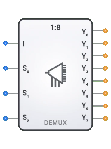
- Symbol: Typically represented as a rectangular block with one data input (DATA), three select inputs (S0-S2), and eight outputs (Y0-Y7).
- DigiSim.io Role: Serves as an essential component for data distribution, address decoding, and control signal routing in digital systems, allowing selective transmission of signals to multiple destinations.
Functional Description
Logic Behavior
The 1-to-8 Demultiplexer directs the input data to a specific output line indicated by the binary value on its select inputs. Only one output (corresponding to the select line values) receives the input data, while all other outputs remain inactive. If the input data is LOW, all outputs remain LOW regardless of select values.
Truth Table:
| S2 | S1 | S0 | DATA | Y7 | Y6 | Y5 | Y4 | Y3 | Y2 | Y1 | Y0 |
|---|---|---|---|---|---|---|---|---|---|---|---|
| 0 | 0 | 0 | 0 | 0 | 0 | 0 | 0 | 0 | 0 | 0 | 0 |
| 0 | 0 | 0 | 1 | 0 | 0 | 0 | 0 | 0 | 0 | 0 | 1 |
| 0 | 0 | 1 | 1 | 0 | 0 | 0 | 0 | 0 | 0 | 1 | 0 |
| 0 | 1 | 0 | 1 | 0 | 0 | 0 | 0 | 0 | 1 | 0 | 0 |
| 0 | 1 | 1 | 1 | 0 | 0 | 0 | 0 | 1 | 0 | 0 | 0 |
| 1 | 0 | 0 | 1 | 0 | 0 | 0 | 1 | 0 | 0 | 0 | 0 |
| 1 | 0 | 1 | 1 | 0 | 0 | 1 | 0 | 0 | 0 | 0 | 0 |
| 1 | 1 | 0 | 1 | 0 | 1 | 0 | 0 | 0 | 0 | 0 | 0 |
| 1 | 1 | 1 | 1 | 1 | 0 | 0 | 0 | 0 | 0 | 0 | 0 |
Note: When DATA = 0, all outputs remain at 0 regardless of select values.
Inputs and Outputs
Inputs:
- DATA: 1-bit input signal to be routed to one of the eight outputs.
- S0: Least Significant Bit (LSB) of the 3-bit select input.
- S1: Middle bit of the 3-bit select input.
- S2: Most Significant Bit (MSB) of the 3-bit select input.
Outputs:
- Y0-Y7: Eight 1-bit outputs, only one of which can be active at a time when enabled. The specific active output is determined by the binary value of S2, S1, and S0.
Configurable Parameters
- Output Logic: Whether outputs are active-high or active-low.
- Enable Logic: Whether the enable input is active-high or active-low.
- Multiple Enables: Some implementations support multiple enable inputs (with AND/OR functionality).
- Output Type: Standard, open-collector, or open-drain output configurations.
- Propagation Delay: The time it takes for outputs to change after input changes.
Visual Representation in DigiSim.io
The 1-to-8 Demultiplexer is displayed as a rectangular block with input pins on the left side (DATA, S0, S1, S2) and eight output pins (Y0-Y7) on the right side. When connected in a circuit, the component visually indicates the active data path through color changes on connecting wires.
Educational Value
Key Concepts
- Signal Distribution: Demonstrates how digital systems route a single signal to multiple possible destinations.
- Binary Addressing: Shows how binary codes can select specific output channels.
- Selective Activation: Illustrates how a system can activate one of many components based on an address.
- Data Routing: Presents fundamental concepts of signal routing and channel selection.
- Inverse Multiplexing: Demonstrates the complementary operation to multiplexing.
Learning Objectives
- Understand how demultiplexers route signals based on select line values.
- Learn the relationship between binary codes and activated outputs.
- Recognize how demultiplexers can be used for address decoding and data distribution.
- Apply demultiplexer concepts in creating larger digital systems.
- Comprehend the duality between multiplexers and demultiplexers in digital design.
- Develop skills in signal routing and distribution in digital circuits.
Usage Examples/Scenarios
- Memory Addressing: Selecting one of eight memory chips based on address bits.
- I/O Port Expansion: Distributing control signals to multiple peripheral devices.
- Parallel Data Generation: Converting serial data to parallel by routing each bit to different outputs over time.
- Control Signal Distribution: Directing control signals to specific subsystems based on operation codes.
- Channel Selection: Routing audio or data signals to specific output channels.
- Selective Component Activation: Enabling one of multiple similar components for power efficiency.
- Serial-to-Parallel Conversion: Distributing sequential bits to parallel outputs in communication systems.
Technical Notes
- The 1-to-8 demultiplexer can be implemented using a 3-to-8 decoder followed by AND gates.
- Each output line follows the boolean function: Y(n) = DATA • EN • (S2, S1, S0 == n).
- Common IC implementations include the 74138 with additional AND gates for the data input.
- Cascading two 1-to-4 demultiplexers with an additional select bit can create a 1-to-8 demultiplexer.
- The propagation delay is typically 10-25ns in standard IC implementations, depending on technology.
- In DigiSim.io, the demultiplexer accurately models the operation of standard demultiplexer circuits, showing proper signal routing based on select inputs.
Characteristics
Input Configuration:
- One data input (DATA)
- Three select inputs (S0, S1, S2)
- Optional enable input (EN)
- Input loading consistent with logic family used
- Standard logic levels (typically TTL or CMOS compatible)
- May include active-low enable in some implementations
- May include multiple enable inputs (AND/OR function)
- Input protection against static discharge typical
Output Configuration:
- Eight mutually exclusive outputs (Y0-Y7)
- Active-high or active-low outputs depending on implementation
- Only one output active at a time (when DATA = 1)
- All outputs inactive when demultiplexer is disabled
- All outputs inactive when DATA = 0 (regardless of select values)
- Capable of driving standard digital loads
- May include open-collector/open-drain variants
- Output loading affects propagation delay
Functionality:
- Routes single input to one of eight outputs
- Select lines determine which output receives the input
- Enable input controls overall operation
- Combinational logic operation (no clock required)
- Can be cascaded for more outputs
- Binary-to-one-hot distribution
- Often used with active-low outputs in bus systems
- Output determined solely by current input state
Propagation Delay:
- Data input to output: 7-20ns typical
- Select input to output: 10-25ns typical
- Enable to output: 8-22ns typical
- Technology dependent (TTL, CMOS, etc.)
- Consistent delay across all output paths is desirable
- Critical parameter in high-speed data distribution
- Affected by output loading
- Temperature and voltage sensitive
Fan-Out:
- Each output typically drives 10-20 standard loads
- Output current capability defined by logic family
- May require buffering for high fan-out situations
- Active output must provide sufficient drive for target devices
- Consistent with logic family specifications
- May vary between devices in same family
- Critical for reliable signal distribution
Power Consumption:
- Low to moderate power requirements
- Static power minimal in CMOS implementations
- Dynamic power increases with switching frequency
- Proportional to switching activity
- Technology dependent (CMOS lowest static power)
- Power increases with fan-out loading
- Typical values: 5-25mW active, <1mW standby (CMOS)
Circuit Complexity:
- Moderate complexity
- Implemented with basic logic gates
- AND-based or NAND-based implementations common
- Decoder followed by AND gates structure
- Additional logic for enable function
- Integrated implementations reduce external component count
- Minimal complexity compared to functionality provided
Implementation Methods
Decoder-Based Implementation
- Built from 3-to-8 decoder and AND gates
- Decoder converts select lines to one-hot format
- Each output uses an AND gate with decoder output and data input
- Enable signal controls the decoder
- Most common and straightforward implementation
- Clear functional separation between addressing and data
- Educational example of demultiplexing principles
- Can leverage existing decoder components
Gate-Level Direct Implementation
- Built directly from basic logic gates (AND, NOT)
- Each output requires a 4-input AND gate (3 select inputs + data)
- Input inverters generate complement signals as needed
- No intermediate decoder stage
- More gates but potentially faster than decoder-based
- Direct implementation of demultiplexer function
- Useful for understanding fundamental operation
- Regular structure simplifies layout
Integrated Circuit Implementation
- Dedicated demultiplexer ICs: 74xx138 with AND gates
- Various features: enables, latches, open-collector
- Available in different logic families
- Well-characterized timing and loading
- Standard interfaces and pinouts
- Often used in data distribution and control signal routing
- Multiple enable inputs for cascading
- Cost-effective, space-efficient solution
Transmission Gate Implementation
- Uses CMOS transmission gates as switches
- Lower propagation delay than gate-level approach
- Efficient in CMOS technology
- Lower power consumption
- More sensitive to signal integrity issues
- Requires careful design
- Common in modern CMOS integrated circuits
- Well-suited for ASIC/FPGA implementation
Multiplexer-Derived Implementation
- Using multiplexer with restructured connections
- Connect data input to all multiplexer inputs
- Select lines control which path is active
- Can leverage available multiplexer components
- Demonstrates duality between multiplexers and demultiplexers
- Alternative approach when demultiplexers not available
- May have different timing characteristics
- Useful in resource-constrained designs
FPGA/ASIC Implementation
- Implemented using LUTs or dedicated resources
- Optimized for target technology
- Synthesized from HDL descriptions
- Can incorporate additional features
- Resource utilization optimized by tools
- Performance customizable based on requirements
- Can be deeply integrated with other logic
- Modern implementation approach for complex systems
Tree-Structure Implementation
- Hierarchical structure of 1-to-2 demultiplexers
- First level uses S2, second S1, third S0
- Logarithmic delay characteristics
- Modular, scalable design
- Can be more efficient in some technologies
- Uniform delay across all outputs
- Educational value in demonstrating decomposition
- Building block approach to complex functions
Applications
Data Distribution
- Routing control signals to multiple destinations
- Bus architecture signal distribution
- Selective activation of subsystems
- Command broadcasting to specific targets
- Configuration signal routing
- Control word distribution
- Protocol-based selective communications
Memory and Storage Systems
- Memory chip selection
- Memory bank enabling
- Write enable signal distribution
- Address space partitioning
- Storage device selection
- Memory-mapped I/O addressing
- Cache line selection
Serial-to-Parallel Conversion
- Converting serial data streams to parallel outputs
- Time-division demultiplexing
- Channel separation
- Bit distribution from serial interfaces
- Protocol decoding
- Frame disassembly
- Sensor data distribution
Display Systems
- Segment driving in multiplexed displays
- Row/column selection in display matrices
- Pixel addressing
- Character position selection
- Display mode control signal routing
- Backlight zone control
- Color channel distribution
Communication Systems
- Channel allocation
- Receiver selection
- Protocol-specific signaling
- Network node addressing
- Data packet routing
- Wireless communication channel selection
- Interface selection in multi-standard systems
Testing and Debugging
- Signal injection at specific test points
- Diagnostic routing
- Selective circuit stimulation
- Error pattern generation
- System validation
- Fault isolation
- Built-in self-test control
Input/Output Expansion
- GPIO pin multiplication
- I/O port expansion
- Peripheral control signal distribution
- Interface signal routing
- Sensor selection
- Actuator control distribution
- External device addressing
Limitations
Signal Distribution Constraints
- Only one output active at a time
- Cannot route data to multiple outputs simultaneously
- Input signal must be valid during selection
- Fan-out limited by output drive capability
- May require buffering for high-load applications
- Propagation delay impacts high-speed applications
- Limited isolation between channels
Timing Considerations
- Select lines must be stable before data valid
- Glitches possible during select line transitions
- Setup and hold time requirements
- Data must remain valid for distribution
- Synchronization with system timing critical
- Select line change to output stabilization delay
- Race conditions in asynchronous systems
Scalability Challenges
- Exponential growth in select lines for linear output increase
- 16 outputs would require 4 select lines
- Large demultiplexers require significant resources
- Pin count limitations for larger implementations
- Cascading introduces additional delay
- Complexity increases dramatically with size
- Testing complexity increases exponentially
Signal Integrity Issues
- Crosstalk between output channels
- Ground bounce in high-speed switching
- Power supply noise during transitions
- Transmission line effects on long traces
- Clock feedthrough in transmission gate implementations
- Signal degradation through multiple stages
- Noise margin reduction at high speeds
Implementation Trade-offs
- Speed vs. power consumption
- Resource usage vs. performance
- Active vs. passive implementations
- Size vs. modularity
- Delay matching vs. component count
- Drive capability vs. integration density
- Custom vs. standard component use
Circuit Implementation Detail
Decoder-Based 1-to-8 Demultiplexer
graph TB
    S0[S0] --> DEC[3-to-8 Decoder]
    S1[S1] --> DEC
    S2[S2] --> DEC
    EN[Enable] --> DEC

    DEC -->|Y0'| AND0[AND]
    DEC -->|Y1'| AND1[AND]
    DEC -->|Y2'| AND2[AND]
    DEC -->|Y3'| AND3[AND]
    DEC -->|Y4'| AND4[AND]
    DEC -->|Y5'| AND5[AND]
    DEC -->|Y6'| AND6[AND]
    DEC -->|Y7'| AND7[AND]

    DATA[Data Input] --> AND0
    DATA --> AND1
    DATA --> AND2
    DATA --> AND3
    DATA --> AND4
    DATA --> AND5
    DATA --> AND6
    DATA --> AND7

    AND0 --> Y0[Y0 Output]
    AND1 --> Y1[Y1 Output]
    AND2 --> Y2[Y2 Output]
    AND3 --> Y3[Y3 Output]
    AND4 --> Y4[Y4 Output]
    AND5 --> Y5[Y5 Output]
    AND6 --> Y6[Y6 Output]
    AND7 --> Y7[Y7 Output]
Operation: Decoder selects one output line based on S2:S1:S0, AND gates route DATA to selected output.
Gate-Level Direct Implementation (Y0 Output Only)
graph LR
    Select0[S0] --> NotGate0[NOT]
    Select1[S1] --> NotGate1[NOT]
    Select2[S2] --> NotGate2[NOT]

    NotGate0 --> AndGate[AND Gate]
    NotGate1 --> AndGate
    NotGate2 --> AndGate
    DataIn[Data] --> AndGate
    EnablePin[Enable] --> AndGate

    AndGate --> OutputY0[Y0 Output]
Logic for Y0: Y0 = DATA · /S2 · /S1 · /S0 · Enable (active when S2:S1:S0 = 000)
74HC138 + 74HC08 Implementation
Configuration:
| Component | Input | Output | Connection |
|---|---|---|---|
| 74HC138 | A, B, C | Y0-Y7 | Select inputs S0-S2 |
| 74HC138 | G1, /G2A, /G2B | Enable | G1=1, /G2A=0, /G2B=0 |
| 74HC08 | 1A-4A, 1B-4B | 1Y-4Y | AND decoder outputs with DATA |
Implementation:
graph LR
    S[S2:S1:S0] --> DEC[74HC138 Decoder]
    DEC --> AND[74HC08 Quad AND]
    DATA[Data Input] --> AND
    AND --> OUT[Y0-Y7 Outputs]
Operation: 74HC138 decodes address, 74HC08 ANDs decoder outputs with DATA signal.
Note: G1 is active-high and G2A, G2B are active-low enable inputs on the 74HC138. For a 1-to-8 demultiplexer, tie G1 to logic 1, and G2A and G2B to logic 0 or use them as enable inputs.
Related Components
- 1-to-2 Demultiplexer: Simplest demultiplexer with one select line
- 1-to-4 Demultiplexer: Medium-sized demultiplexer with two select lines
- 1-to-16 Demultiplexer: Larger demultiplexer with four select lines
- 3-to-8 Decoder: Component often used in demultiplexer implementations
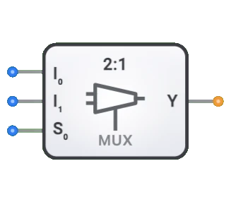
- 8-to-1 Multiplexer: Performs the inverse operation of a 1-to-8 demultiplexer
- Data Distributor: Alternative name for demultiplexer in certain applications
- Serial-to-Parallel Converter: Uses demultiplexing principles for conversion
- Bus Demultiplexer: Specialized for bus data distribution
- Channel Demultiplexer: Used in communication systems for channel separation
- Address Decoder: Related component used for memory and I/O addressing