3-to-8 Decoder
Overview
- Purpose: The 3-to-8 Decoder is a digital combinational circuit that converts a 3-bit binary input code into eight mutually exclusive output lines, activating exactly one output line based on the input value.
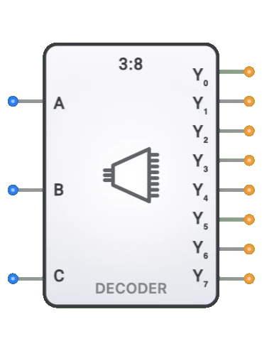
- Symbol: Typically represented as a rectangular block with three binary inputs (A0, A1, A2), one enable input (EN), and eight outputs (Y0-Y7).
- DigiSim.io Role: Serves as an essential building block in digital systems for address decoding, memory selection, data demultiplexing, and control signal generation.
Functional Description
Logic Behavior
The 3-to-8 Decoder "decodes" the binary information into a one-hot output format, where only one of the eight possible output lines is active for each unique input combination. When enabled, the output line corresponding to the binary value of the input is activated, while all other outputs remain inactive.
Truth Table:
| Enable | A2 | A1 | A0 | Y7 | Y6 | Y5 | Y4 | Y3 | Y2 | Y1 | Y0 |
|---|---|---|---|---|---|---|---|---|---|---|---|
| 0 | X | X | X | 0 | 0 | 0 | 0 | 0 | 0 | 0 | 0 |
| 1 | 0 | 0 | 0 | 0 | 0 | 0 | 0 | 0 | 0 | 0 | 1 |
| 1 | 0 | 0 | 1 | 0 | 0 | 0 | 0 | 0 | 0 | 1 | 0 |
| 1 | 0 | 1 | 0 | 0 | 0 | 0 | 0 | 0 | 1 | 0 | 0 |
| 1 | 0 | 1 | 1 | 0 | 0 | 0 | 0 | 1 | 0 | 0 | 0 |
| 1 | 1 | 0 | 0 | 0 | 0 | 0 | 1 | 0 | 0 | 0 | 0 |
| 1 | 1 | 0 | 1 | 0 | 0 | 1 | 0 | 0 | 0 | 0 | 0 |
| 1 | 1 | 1 | 0 | 0 | 1 | 0 | 0 | 0 | 0 | 0 | 0 |
| 1 | 1 | 1 | 1 | 1 | 0 | 0 | 0 | 0 | 0 | 0 | 0 |
Note: X means "don't care". Some implementations may use active-low outputs or active-low enable, inverting the output logic shown above.
Inputs and Outputs
Inputs:
- A0: Least Significant Bit (LSB) of the 3-bit binary input.
- A1: Middle bit of the 3-bit binary input.
- A2: Most Significant Bit (MSB) of the 3-bit binary input.
- EN: Enable input that controls whether the decoder is active.
Outputs:
- Y0-Y7: Eight mutually exclusive outputs, only one of which is active at a time when the decoder is enabled. Y0 corresponds to binary input 000, Y1 to 001, and so on up to Y7 for 111.
Configurable Parameters
- Output Logic: Whether outputs are active-high or active-low.
- Enable Logic: Whether the enable input is active-high or active-low.
- Multiple Enables: Some implementations support multiple enable inputs (with AND/OR functionality).
- Propagation Delay: The time it takes for outputs to change after input changes.
Visual Representation in DigiSim.io
The 3-to-8 Decoder is displayed as a rectangular block with input pins on the left side (A0, A1, A2, EN) and eight output pins (Y0-Y7) on the right side. When connected in a circuit, the component visually indicates the active output through color changes on connecting wires.
Educational Value
Key Concepts
- Binary Decoding: Demonstrates how digital systems convert compact binary codes into individual control lines.
- One-Hot Encoding: Shows how binary values can be represented in a format where only one bit is active.
- Address Decoding: Illustrates a fundamental technique used in memory and I/O systems.
- Signal Demultiplexing: Presents the concept of directing signals based on binary addressing.
- Combinational Logic: Provides a practical example of combinational circuit design using AND and NOT gates.
Learning Objectives
- Understand how binary values can be decoded into mutually exclusive output signals.
- Learn the relationship between binary addressing and component selection in digital systems.
- Recognize how decoders enable efficient control of multiple subsystems using minimal input lines.
- Apply decoder concepts in memory addressing, peripheral selection, and control signal generation.
- Comprehend how decoders can be cascaded or combined to create larger decoding structures.
Usage Examples/Scenarios
- Memory Chip Selection: Using the decoder to select one of eight memory chips based on address bits.
- I/O Device Addressing: Activating a specific peripheral device from eight possible options.
- Instruction Decoding: Generating control signals based on instruction opcodes in a processor.
- Multiplexed Display Control: Selecting which digit to activate in multi-digit display systems.
- Test Point Selection: Routing a test signal to one of eight possible test points.
- State Machine Implementation: Generating state-specific control signals in a digital controller.
- Data Routing: Directing data to one of eight possible destinations based on a 3-bit selector.
Technical Notes
- The 3-to-8 decoder can be implemented using three inverters and eight 4-input AND gates.
- Each output line follows the boolean function: Y(n) = EN • An • Am • Ak (where n is the output number, and An, Am, Ak are the address bits or their complements).
- Some common IC implementations include the 74138 (3-to-8 decoder with active-low outputs) and 74238 (3-to-8 decoder with active-high outputs).
- Cascading two 3-to-8 decoders with an additional address bit can create a 4-to-16 decoder.
- The propagation delay is typically 10-25ns in standard IC implementations, depending on technology.
- In DigiSim.io, the decoder accurately models the operation of standard decoder ICs with proper output activation.
Characteristics
Input Configuration:
- Three binary address inputs (A0, A1, A2)
- Optional enable input (EN)
- Input loading consistent with logic family used
- Standard logic levels (typically TTL or CMOS compatible)
- May include active-low enable in some implementations
- May include multiple enable inputs (AND/OR function)
- Input protection against static discharge typical
Output Configuration:
- Eight mutually exclusive outputs (Y0-Y7)
- Active-high or active-low outputs depending on implementation
- One-hot encoding (only one output active at a time when enabled)
- All outputs inactive when decoder is disabled
- Capable of driving standard digital loads
- May include open-collector/open-drain variants for wired-OR capability
- Some implementations feature latched outputs
- Output loading affects propagation delay
Functionality:
- Converts 3-bit binary code to one of eight output lines
- Mutually exclusive outputs (one-hot encoding)
- Enable input controls overall operation
- Combinational logic operation (no clock required)
- Can be cascaded for larger decoders
- Binary-to-unary converter
- Often used with active-low outputs for chip selection
- Output determined solely by current input state
Propagation Delay:
- Input to output: 7-20ns typical
- Enable to output: 8-25ns typical
- Technology dependent (TTL, CMOS, etc.)
- Consistent delay across all output lines is desirable
- Critical parameter in high-speed memory systems
- Affected by output loading
- Temperature and voltage sensitive
- Affects system timing and address setup requirements
Fan-Out:
- Typically drives 10-20 standard loads
- Output current capability defined by logic family
- May require buffering for high fan-out situations
- Critical parameter for chip select applications
- Active outputs must provide sufficient drive for target devices
- Consistent with logic family specifications
- May vary between devices in same family
Power Consumption:
- Low to moderate power requirements
- Static power minimal in CMOS implementations
- Dynamic power increases with switching frequency
- Proportional to number of active outputs
- Technology dependent (CMOS lowest static power)
- Power increases with fan-out loading
- Typical values: 5-25mW active, <1mW standby (CMOS)
Circuit Complexity:
- Moderate complexity
- Implemented with basic logic gates
- AND-based or NAND-based implementations common
- Requires 8 separate decode paths
- Additional logic for enable function
- Integrated implementations reduce external component count
- Minimal complexity compared to functionality provided
Implementation Methods
Gate-Level Implementation
- Built from basic logic gates (AND, NOT)
- Each output requires a 4-input AND gate (3 address inputs + enable)
- Input inverters generate complement signals as needed
- Enable signal common to all outputs
- Direct implementation of decoder function
- Clear educational example of decoder operation
- Straightforward but requires many gates
- Regular structure simplifies layout
NAND/NOR Implementation
- Uses NAND or NOR gates with appropriate inversions
- Often more efficient in certain logic families
- May produce active-low outputs naturally
- Common in TTL implementations
- Leverages common gate types in technology
- Can reduce component count
- May offer improved performance
- Standard approach in many integrated circuits
Integrated Circuit Implementation
- Dedicated decoder ICs: 74xx138 (3-to-8 decoder)
- Various features: enables, latches, open-collector
- Available in different logic families
- Well-characterized timing and loading
- Standard interfaces and pinouts
- Often used in memory and peripheral address decoding
- Multiple enable inputs for cascading
- Cost-effective, space-efficient solution
Cascaded 2-to-4 Decoders
- Two 2-to-4 decoders with enable control
- MSB selects which decoder is active
- More modular approach
- Uses smaller, common components
- Potentially useful when 2-to-4 decoders are already available
- Two-level decoding may have timing implications
- Demonstrates principles of decoder cascading
- Building block for larger decoders
PLA/ROM Implementation
- Programmable Logic Array approach
- Uses AND-OR structure
- Utilized in FPGA and CPLD implementations
- Configurable for various decoding schemes
- Flexible for custom addressing schemes
- More complex but highly versatile
- Common in modern programmable devices
- Can be optimized for speed or resource usage
Demultiplexer-Based Implementation
- 1-to-8 demultiplexer with input tied high
- Address inputs control routing
- Functionally equivalent to decoder
- Alternative perspective on decoder function
- Can leverage existing demultiplexer components
- Illustrates relationship between decoding and demultiplexing
- May offer design or resource advantages in certain contexts
Multiplexer-Based Implementation
- Configured multiplexers can implement decoder functions
- Less intuitive but versatile approach
- Common in FPGA implementations
- Leverages available resources efficiently
- May be preferred when multiplexers are abundant
- Demonstrates functional equivalence of different structures
- Advanced implementation technique
Applications
Memory Address Decoding
- RAM/ROM chip selection
- Memory bank activation
- Address space partitioning
- Memory-mapped I/O selection
- Cache way selection
- Page selection
- Memory interleaving control
Peripheral Device Selection
- I/O device addressing
- Peripheral chip selects
- Bus slave selection
- Port addressing
- Device multiplexing
- Channel selection
- Hardware resource allocation
Instruction Decoding
- CPU instruction decoding
- Opcode decoding
- Microcode addressing
- Execution unit selection
- State machine implementation
- Control signal generation
- Operation selection
Demultiplexing
- Data routing control
- Channel selection
- Output port direction
- Signal distribution
- Bus routing
- Data path control
- Selective broadcasting
Control Signal Generation
- Sequencer implementation
- State machine outputs
- Control word generation
- Timing signal creation
- Selective reset/preset
- Mode selection
- System configuration
Display Systems
- Display digit selection
- LED matrix row/column driving
- LCD segment selection
- Display memory addressing
- Character generator addressing
- Display mode control
- Segment decoder
Testing and Debugging
- Test point selection
- Diagnostic output routing
- Debug signal selection
- Built-in self-test control
- Scan chain control
- Error code generation
- Fault isolation
Limitations
Fan-Out Restrictions
- Limited current drive capability
- May require buffering for high-load applications
- Active outputs must drive all connected devices
- Heavily loaded outputs have increased delay
- Can limit maximum operating speed
- Critical in chip select applications
- May require additional buffer stages
Propagation Delay Implications
- Address setup time requirements
- Limits maximum operating frequency
- Critical path in memory access timing
- Can introduce timing hazards
- Address change to output stabilization delay
- Cascaded decoders have increased delay
- Affects system clock rate in synchronous designs
Power Consumption Considerations
- Significant when many outputs change simultaneously
- Increases with operating frequency
- Becomes critical in battery-operated devices
- May cause supply voltage droop during transitions
- Ground bounce in high-speed applications
- Thermal management in high-speed systems
- Power spikes during address transitions
Scalability Challenges
- Exponential growth in outputs with linear input increase
- Large decoders require significant resources
- Pin count limitations for larger decoders
- Cascading introduces additional delay
- Complexity increases dramatically with size
- Power consumption grows with size
- Testing complexity increases exponentially
Operational Hazards
- Glitches during input transitions
- Multiple outputs momentarily active during transitions
- Address setup and hold time violations
- Noise sensitivity on enable inputs
- Partial decoding in large cascaded systems
- Enable signal timing critical
- Race conditions in asynchronous systems
Circuit Implementation Detail
Basic 3-to-8 Decoder with AND Gates
graph TB
    A0[A0] --> NOT0[NOT]
    A1[A1] --> NOT1[NOT]
    A2[A2] --> NOT2[NOT]
    EN[Enable]

    NOT0 --> AND0[AND]
    NOT1 --> AND0
    NOT2 --> AND0
    EN --> AND0
    AND0 --> Y0[Y0: 000]

    A0 --> AND1[AND]
    NOT1 --> AND1
    NOT2 --> AND1
    EN --> AND1
    AND1 --> Y1[Y1: 001]

    NOT0 --> AND2[AND]
    A1 --> AND2
    NOT2 --> AND2
    EN --> AND2
    AND2 --> Y2[Y2: 010]

    A0 --> AND3[AND]
    A1 --> AND3
    NOT2 --> AND3
    EN --> AND3
    AND3 --> Y3[Y3: 011]

    NOT0 --> AND4[AND]
    NOT1 --> AND4
    A2 --> AND4
    EN --> AND4
    AND4 --> Y4[Y4: 100]

    A0 --> AND7[AND]
    A1 --> AND7
    A2 --> AND7
    EN --> AND7
    AND7 --> Y7[Y7: 111]
Logic: Each output is active when its corresponding 3-bit address pattern is present and enabled.
74HC138 3-to-8 Decoder Integrated Circuit
Pin Configuration:
| Pin Group | Signal | Function |
|---|---|---|
| Inputs | A, B, C | Address inputs (A0-A2) |
| Enables | G1 | Active-HIGH enable |
| Enables | /G2A, /G2B | Active-LOW enables |
| Outputs | Y0-Y7 | Active-LOW outputs |
| Power | Vcc, GND | +5V and Ground |
Enable Condition: Decoder active when G1=1 AND /G2A=0 AND /G2B=0
Output Selection: Only one output is LOW at a time based on C:B:A address
Note: The 74HC138 has active-low outputs (Y0-Y7) and three enable inputs: G1 (active-high), G2A and G2B (both active-low). The decoder is enabled when G1=1, G2A=0, and G2B=0.
Related Components
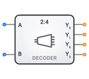
- 2-to-4 Decoder: Smaller decoder with two inputs and four outputs
- 4-to-16 Decoder: Larger decoder with four inputs and sixteen outputs
- Binary-to-7-Segment Decoder: Converts binary values to 7-segment display patterns
- BCD-to-Decimal Decoder: Converts Binary Coded Decimal to ten outputs
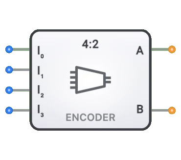
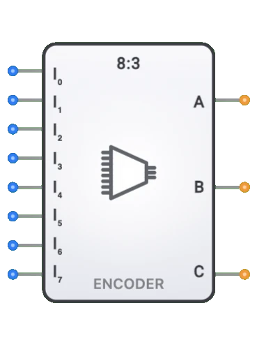
- Priority Encoder: Inverse operation, converts one-hot to binary with priority
- Demultiplexer: Routes one input to one of multiple outputs
- Address Decoder: Specialized decoder for memory addressing
- Instruction Decoder: Specialized decoder for CPU instruction processing
- Bus Decoder: Used for bus address decoding in computer systems
- Binary-to-Gray Code Converter: Related conversion component in digital systems