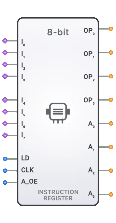
Memory Address Register (MAR)
Overview
- Purpose: The Memory Address Register (MAR) is an 8-bit register that holds the memory address for read/write operations. It acts as a buffer between the CPU's internal address sources (Program Counter, Instruction Register) and the external memory address bus, enabling proper timing and isolation of address signals.
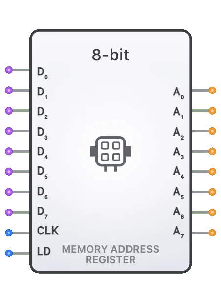
- Symbol: The MAR is represented by a rectangular block with an 8-bit data input bus, clock (CLK) input, load enable (LD) control signal, and an 8-bit address output bus.
- DigiSim.io Role: Essential component in CPU designs that separates address generation from memory access, enabling proper bus timing and supporting complex addressing modes in the 8-bit computer architecture.
Functional Description
Logic Behavior
The Memory Address Register latches an 8-bit address value on the rising edge of the CLK signal when the load enable (LD) is HIGH. This design is consistent with other synchronous registers in the DigiSim 8-bit computer architecture. Once latched, the address is continuously driven on the output pins until a new address is loaded. Unlike tri-state components, the MAR always drives its outputs.
Function Table:
| CLK Edge | LD | Operation | A0-A7 Output |
|---|---|---|---|
| ↑ | 1 | Latch New Address | D0-D7 Input Data |
| ↑ | 0 | Hold | Previous Address |
| - | X | Hold | Previous Address |
Note: ↑ represents a rising edge on CLK signal LD must be HIGH at the rising clock edge to latch new data The outputs are always driven (not tri-state) to ensure stable address bus
Inputs and Outputs
Inputs (10 total):
- D0-D7[7:0]: 8-bit data inputs (bus inputs) for loading a new address. These are configured as bus inputs, allowing multiple sources to drive them through tri-state buffers.
- CLK: Clock input (rising edge triggered). Data is latched on the rising edge of CLK when LD is HIGH.
- LD: 1-bit load enable input (level sensitive). Must be HIGH at the rising CLK edge to latch new data.
Outputs (8 total):
- A0-A7[7:0]: 8-bit address outputs that connect to memory components (RAM/ROM). These outputs are always driven (not tri-state).
Pin Layout
Input Pins (Left Side):
- Pins 0-7: D0-D7 (Data/Address inputs - bus inputs)
- Pin 8: CLK (Clock - rising edge triggered)
- Pin 9: LD (Load Enable - level sensitive)
Output Pins (Right Side):
- Pins 0-7: A0-A7 (Address outputs to memory)
Configurable Parameters
- Initial Value: The address value at power-on (typically 0x00).
- Edge Sensitivity: Rising edge triggered on CLK signal (when LD is HIGH).
- Propagation Delay: The time from CLK rising edge to stable outputs.
Visual Representation in DigiSim.io
The Memory Address Register is displayed as a rectangular block (128×192 pixels, 8×12 grids) with:
- 8 data input pins on the left side (D0-D7) at relativeY: 0.16667 to 0.75
- 1 clock input pin (CLK) at relativeY: 0.83333
- 1 load enable pin (LD) at relativeY: 0.91667
- 8 address output pins on the right side (A0-A7) at relativeY: 0.25 to 0.83333
The component label "MAR" is displayed in the center, with "ADDR" indicating its role as an address register. Input pins are marked as bus inputs, indicated by thicker connection points that can accept multiple tri-state drivers.
Educational Value
Key Concepts
- Address Buffering: Demonstrates how addresses are isolated from their sources for proper bus timing.
- Edge-Triggered Latching: Shows how data is captured on clock/control signal edges.
- Bus Architecture: Illustrates the separation of address and data buses in CPU design.
- Memory Addressing: Fundamental concept in computer architecture.
- Pipeline Stages: The MAR represents a stage in the fetch-decode-execute pipeline.
Learning Objectives
- Understand the role of address registers in memory operations.
- Learn how address buffering enables complex memory access patterns.
- Recognize the timing requirements for memory address setup and hold.
- Apply MAR concepts in designing CPU memory interfaces.
- Comprehend how multiple address sources (PC, IR, ALU) can share a single memory address bus.
Usage Examples/Scenarios
- Instruction Fetch: PC value is loaded into MAR before fetching instruction from ROM/RAM.
- Data Load/Store: Operand address from IR is loaded into MAR for data memory access.
- Indirect Addressing: Calculated addresses from ALU are loaded for pointer-based access.
- Stack Operations: Stack pointer value is loaded for push/pop operations.
- DMA Operations: External address sources can load values for direct memory access.
Integration in 8-Bit Computer
In the DigiSim 8-bit computer architecture, the MAR serves as the central address buffer:
┌─────────────────────────────────────────────────────────────┐
│                     ADDRESS SOURCES                          │
│  ┌────────┐   ┌─────────────────┐   ┌──────────────┐       │
│  │   PC   │   │       IR        │   │     ALU      │       │
│  │ (8-bit)│   │ (4-bit address) │   │  (computed)  │       │
│  └───┬────┘   └───────┬─────────┘   └──────┬───────┘       │
│      │                │                     │                │
│      ▼                ▼                     ▼                │
│  ┌───────────────────────────────────────────────┐          │
│  │              TRI-STATE BUFFERS                │          │
│  │         (controlled by Control Unit)          │          │
│  └───────────────────────┬───────────────────────┘          │
│                          │                                   │
│                          ▼                                   │
│                    ┌───────────┐                            │
│                    │    MAR    │◄──── LD (from CU)          │
│                    │  (8-bit)  │                            │
│                    └─────┬─────┘                            │
│                          │                                   │
│                          ▼                                   │
│                   ┌──────────────┐                          │
│                   │  RAM / ROM   │                          │
│                   └──────────────┘                          │
└─────────────────────────────────────────────────────────────┘
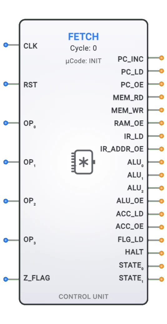
Control Signals
The Control Unit generates the MAR_LD signal during specific microcode steps:
- FETCH state: Load PC value to read next instruction (MAR_LD=1 at CLK rising edge)
- EXECUTE state: Load operand address for memory operations (MAR_LD=1 at CLK rising edge)
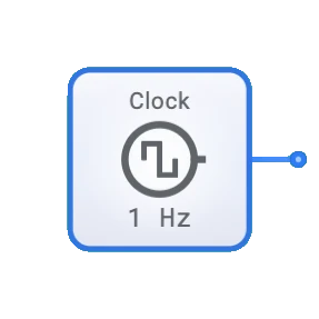
The CLK signal is the system clock shared with all synchronous components.
Technical Notes
- The MAR enables full 8-bit addressing (256 bytes) compared to the 4-bit address output of the Instruction Register.
- Bus inputs allow multiple tri-state sources to connect without explicit multiplexing.
- Rising-edge clock triggering ensures clean address transitions without glitches.
- Outputs are always driven to maintain stable address bus during memory access.
- The MAR should be loaded before asserting memory read/write signals.
- Propagation delay should be accounted for in timing-critical designs.
- The clock input (CLK) synchronizes the MAR with other CPU components.
Related Components
- Program Counter (PC): Primary source of addresses during instruction fetch.
- Instruction Register (IR): Provides operand addresses for memory operations.
- RAM: Random Access Memory addressed by MAR outputs.
- ROM: Read-Only Memory addressed by MAR outputs.
- Control Unit: Generates the LD signal at appropriate times.
- Data Bus: Separate bus for data transfer to/from memory.
- Tri-State Buffer: Used to gate different address sources onto the MAR inputs.